- 您现在的位置:买卖IC网 > PDF目录11590 > PIC16F676-E/P (Microchip Technology)IC MCU FLASH 1KX14 W/AD 14DIP PDF资料下载
参数资料
| 型号: | PIC16F676-E/P |
| 厂商: | Microchip Technology |
| 文件页数: | 74/132页 |
| 文件大小: | 0K |
| 描述: | IC MCU FLASH 1KX14 W/AD 14DIP |
| 产品培训模块: | Asynchronous Stimulus |
| 标准包装: | 30 |
| 系列: | PIC® 16F |
| 核心处理器: | PIC |
| 芯体尺寸: | 8-位 |
| 速度: | 20MHz |
| 外围设备: | 欠压检测/复位,POR,WDT |
| 输入/输出数: | 12 |
| 程序存储器容量: | 1.75KB(1K x 14) |
| 程序存储器类型: | 闪存 |
| EEPROM 大小: | 128 x 8 |
| RAM 容量: | 64 x 8 |
| 电压 - 电源 (Vcc/Vdd): | 2 V ~ 5.5 V |
| 数据转换器: | A/D 8x10b |
| 振荡器型: | 内部 |
| 工作温度: | -40°C ~ 125°C |
| 封装/外壳: | 14-DIP(0.300",7.62mm) |
| 包装: | 管件 |
| 配用: | DM163029-ND - BOARD PICDEM FOR MECHATRONICS |
第1页第2页第3页第4页第5页第6页第7页第8页第9页第10页第11页第12页第13页第14页第15页第16页第17页第18页第19页第20页第21页第22页第23页第24页第25页第26页第27页第28页第29页第30页第31页第32页第33页第34页第35页第36页第37页第38页第39页第40页第41页第42页第43页第44页第45页第46页第47页第48页第49页第50页第51页第52页第53页第54页第55页第56页第57页第58页第59页第60页第61页第62页第63页第64页第65页第66页第67页第68页第69页第70页第71页第72页第73页当前第74页第75页第76页第77页第78页第79页第80页第81页第82页第83页第84页第85页第86页第87页第88页第89页第90页第91页第92页第93页第94页第95页第96页第97页第98页第99页第100页第101页第102页第103页第104页第105页第106页第107页第108页第109页第110页第111页第112页第113页第114页第115页第116页第117页第118页第119页第120页第121页第122页第123页第124页第125页第126页第127页第128页第129页第130页第131页第132页
PIC16F630/676
DS40039F-page 46
2010 Microchip Technology Inc.
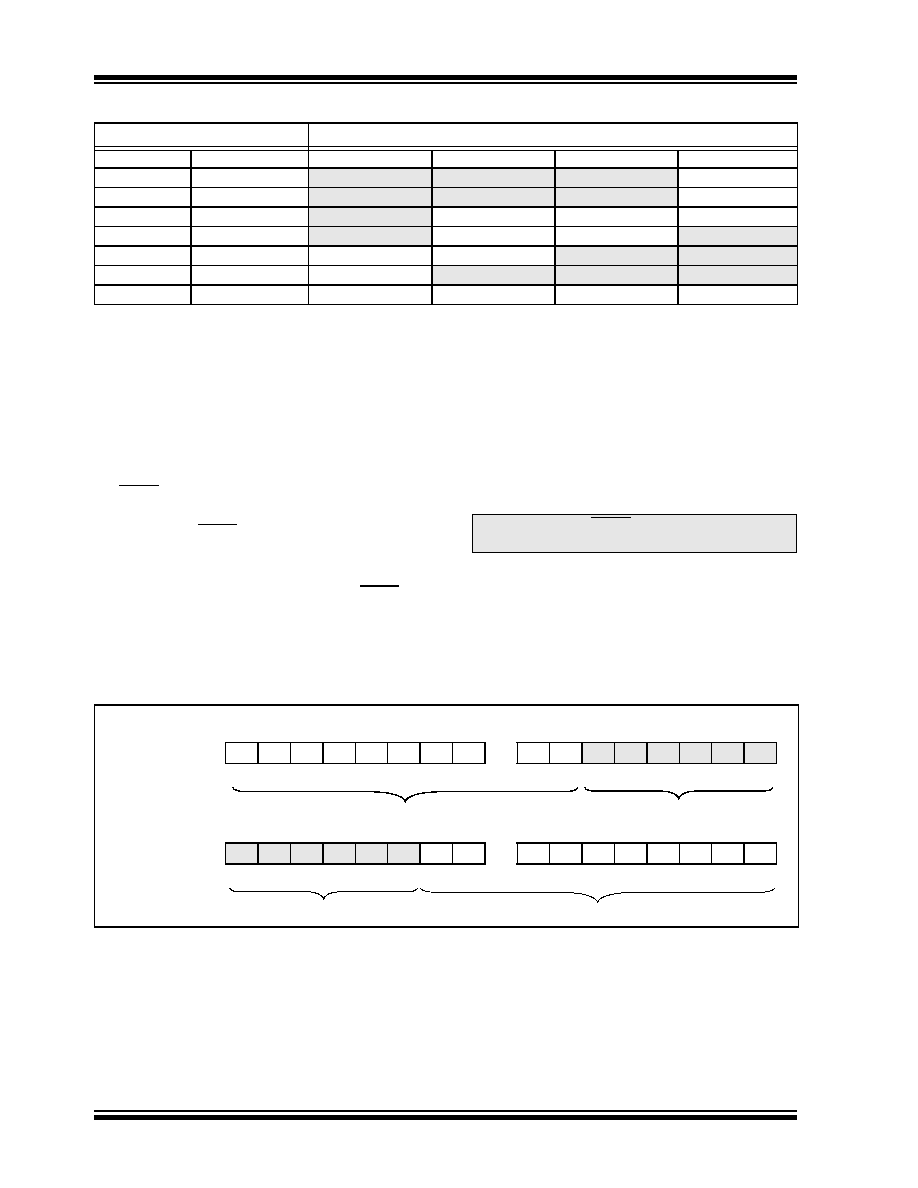
TABLE 7-1:
TAD vs. DEVICE OPERATING FREQUENCIES
7.1.5
STARTING A CONVERSION
The A/D conversion is initiated by setting the
GO/DONE bit (ADCON0<1>). When the conversion is
complete, the A/D module:
Clears the GO/DONE bit
Sets the ADIF flag (PIR1<6>)
Generates an interrupt (if enabled)
If the conversion must be aborted, the GO/DONE bit
can be cleared in software. The ADRESH:ADRESL
registers will not be updated with the partially complete
A/D
conversion
sample.
Instead,
the
ADRESH:ADRESL registers will retain the value of the
previous conversion. After an aborted conversion, a
2TAD delay is required before another acquisition can
be initiated. Following the delay, an input acquisition is
automatically started on the selected channel.
7.1.6
CONVERSION OUTPUT
The A/D conversion can be supplied in two formats: left
or right shifted. The ADFM bit (ADCON0<7>) controls
the output format. Figure 7-2 shows the output formats.
FIGURE 7-2:
10-BIT A/D RESULT FORMAT
A/D Clock Source (TAD)
Device Frequency
Operation
ADCS2:ADCS0
20 MHz
5 MHz
4 MHz
1.25 MHz
2 TOSC
000
100 ns(2)
400 ns(2)
500 ns(2)
1.6
s
4 TOSC
100
200 ns(2)
800 ns(2)
1.0
s(2)
3.2
s
8 TOSC
001
400 ns(2)
1.6
s2.0 s6.4 s
16 TOSC
101
800 ns(2)
3.2
s4.0 s
12.8
s(3)
32 TOSC
010
1.6
s6.4 s
8.0
s(3)
25.6
s(3)
64 TOSC
110
3.2
s
12.8
s(3)
16.0
s(3)
51.2
s(3)
A/D RC
x11
2 - 6
s(1,4)
2 - 6
s(1,4)
2 - 6
s(1,4)
2 - 6
s(1,4)
Legend: Shaded cells are outside of recommended range.
Note 1: The A/D RC source has a typical TAD time of 4
s for VDD > 3.0V.
2: These values violate the minimum required TAD time.
3: For faster conversion times, the selection of another clock source is recommended.
4: When the device frequency is greater than 1 MHz, the A/D RC clock source is only recommended if the
conversion will be performed during Sleep.
Note:
The GO/DONE bit should not be set in the
same instruction that turns on the A/D.
ADRESH
ADRESL
(ADFM = 0)MSB
LSB
bit 7bit 0
10-bit A/D Result
Unimplemented: Read as ‘0’
(ADFM = 1)
MSB
LSB
bit 7bit 0
Unimplemented: Read as ‘0’
10-bit A/D Result
相关PDF资料 |
PDF描述 |
|---|---|
| PIC12LCE518-04/SN | IC MCU OTP 512X12 LV W/EE 8SOIC |
| PIC12CE518-04I/SM | IC MCU OTP 512X12 W/EE 8-SOIC |
| PIC16LF1829T-I/ML | MCU PIC 14KB FLASH 20-QFN |
| PIC16F1829T-I/ML | MCU PIC 14K FLASH 1K RAM 20QFN |
| PIC16F716-E/ML | IC PIC MCU FLASH 2KX14 28QFN |
相关代理商/技术参数 |
参数描述 |
|---|---|
| PIC16F676-I/ML | 功能描述:8位微控制器 -MCU 1.75 KB 64 RAM 12I/O RoHS:否 制造商:Silicon Labs 核心:8051 处理器系列:C8051F39x 数据总线宽度:8 bit 最大时钟频率:50 MHz 程序存储器大小:16 KB 数据 RAM 大小:1 KB 片上 ADC:Yes 工作电源电压:1.8 V to 3.6 V 工作温度范围:- 40 C to + 105 C 封装 / 箱体:QFN-20 安装风格:SMD/SMT |
| PIC16F676-I/P | 功能描述:8位微控制器 -MCU 1.75KB 64 RAM 12 I/O Ind Temp PDIP14 RoHS:否 制造商:Silicon Labs 核心:8051 处理器系列:C8051F39x 数据总线宽度:8 bit 最大时钟频率:50 MHz 程序存储器大小:16 KB 数据 RAM 大小:1 KB 片上 ADC:Yes 工作电源电压:1.8 V to 3.6 V 工作温度范围:- 40 C to + 105 C 封装 / 箱体:QFN-20 安装风格:SMD/SMT |
| PIC16F676-I/P | 制造商:Microchip Technology Inc 功能描述:IC 8BIT FLASH MCU 16F676 DIP14 |
| PIC16F676-I/SL | 功能描述:8位微控制器 -MCU 1.75KB 64 RAM 12 I/O Ind Temp SOIC14 RoHS:否 制造商:Silicon Labs 核心:8051 处理器系列:C8051F39x 数据总线宽度:8 bit 最大时钟频率:50 MHz 程序存储器大小:16 KB 数据 RAM 大小:1 KB 片上 ADC:Yes 工作电源电压:1.8 V to 3.6 V 工作温度范围:- 40 C to + 105 C 封装 / 箱体:QFN-20 安装风格:SMD/SMT |
| PIC16F676-I/SL | 制造商:Microchip Technology Inc 功能描述:8BIT FLASH MCU SMD 16F676 SOIC14 |
发布紧急采购,3分钟左右您将得到回复。