- 您现在的位置:买卖IC网 > PDF目录299771 > PIC16LC926-I/PT 8-BIT, OTPROM, 10 MHz, RISC MICROCONTROLLER, PQFP64 PDF资料下载
参数资料
| 型号: | PIC16LC926-I/PT |
| 元件分类: | 微控制器/微处理器 |
| 英文描述: | 8-BIT, OTPROM, 10 MHz, RISC MICROCONTROLLER, PQFP64 |
| 封装: | 10 X 10 MM, 1 MM HEIGHT, PLASTIC, TQFP-64 |
| 文件页数: | 111/183页 |
| 文件大小: | 3233K |
| 代理商: | PIC16LC926-I/PT |
第1页第2页第3页第4页第5页第6页第7页第8页第9页第10页第11页第12页第13页第14页第15页第16页第17页第18页第19页第20页第21页第22页第23页第24页第25页第26页第27页第28页第29页第30页第31页第32页第33页第34页第35页第36页第37页第38页第39页第40页第41页第42页第43页第44页第45页第46页第47页第48页第49页第50页第51页第52页第53页第54页第55页第56页第57页第58页第59页第60页第61页第62页第63页第64页第65页第66页第67页第68页第69页第70页第71页第72页第73页第74页第75页第76页第77页第78页第79页第80页第81页第82页第83页第84页第85页第86页第87页第88页第89页第90页第91页第92页第93页第94页第95页第96页第97页第98页第99页第100页第101页第102页第103页第104页第105页第106页第107页第108页第109页第110页当前第111页第112页第113页第114页第115页第116页第117页第118页第119页第120页第121页第122页第123页第124页第125页第126页第127页第128页第129页第130页第131页第132页第133页第134页第135页第136页第137页第138页第139页第140页第141页第142页第143页第144页第145页第146页第147页第148页第149页第150页第151页第152页第153页第154页第155页第156页第157页第158页第159页第160页第161页第162页第163页第164页第165页第166页第167页第168页第169页第170页第171页第172页第173页第174页第175页第176页第177页第178页第179页第180页第181页第182页第183页
2001 Microchip Technology Inc.
Preliminary
DS39544A-page 31
PIC16C925/926
4.2
PORTB and TRISB Register
PORTB is an 8-bit wide, bi-directional port. The corre-
sponding data direction register is TRISB. Setting a bit
in the TRISB register puts the corresponding output
driver in a Hi-Impedance Input mode. Clearing a bit in
the TRISB register puts the contents of the output latch
on the selected pin(s).
EXAMPLE 4-2:
INITIALIZING PORTB
Each of the PORTB pins has a weak internal pull-up. A
single control bit can turn on all the pull-ups. This is per-
formed by clearing bit RBPU (OPTION<7>). The weak
pull-up is automatically turned off when the port pin is
configured as an output. The pull-ups are also disabled
on a Power-on Reset.
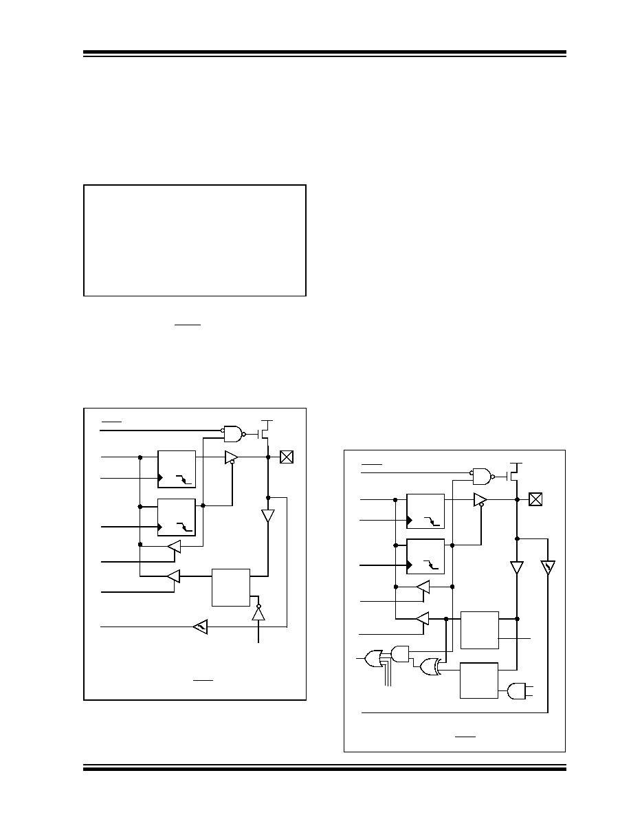
FIGURE 4-3:
BLOCK DIAGRAM OF
RB3:RB0 PINS
Four
of
the
PORTB
pins
(RB7:RB4)
have
an
interrupt-on-change feature. Only pins configured as
inputs can cause this interrupt to occur (i.e., any
RB7:RB4 pin configured as an output is excluded from
the interrupt-on-change comparison). The input pins (of
RB7:RB4) are compared with the old value latched on
the last read of PORTB. The “mismatch” outputs of
RB7:RB4 are OR’ed together to generate the RB Port
Change Interrupt with flag bit RBIF (INTCON<0>).
This interrupt can wake the device from SLEEP. The
user, in the Interrupt Service Routine, can clear the
interrupt in the following manner:
a)
Any read or write of PORTB. This will end the
mismatch condition.
b)
Clear flag bit RBIF.
A mismatch condition will continue to set flag bit RBIF.
Reading PORTB will end the mismatch condition, and
allow flag bit RBIF to be cleared.
This interrupt-on-mismatch feature, together with soft-
ware configurable pull-ups on these four pins, allow easy
interface to a keypad and make it possible for wake-up on
key depression. Refer to the Embedded Control Hand-
book, “Implementing Wake-Up on Key Stroke” (AN552).
The interrupt-on-change feature is recommended for
wake-up on key depression operation and operations
where PORTB is only used for the interrupt-on-change
feature. Polling of PORTB is not recommended while
using the interrupt-on-change feature.
FIGURE 4-4:
BLOCK DIAGRAM OF
RB7:RB4 PINS
BCF
STATUS, RP0
; Select Bank0
BCF
STATUS, RP1
CLRF
PORTB
; Initialize PORTB
BSF
STATUS, RP0
; Select Bank1
MOVLW
0xCF
; Value used to
; initialize data
; direction
MOVWF
TRISB
; Set RB<3:0> as inputs
; RB<5:4> as outputs
; RB<7:6> as inputs
Data Latch
RBPU(2)
P
VDD
Q
D
CK
Q
D
CK
QD
EN
Data Bus
WR Port
WR TRIS
RD TRIS
RD Port
Weak
Pull-up
RD Port
RB0/INT
I/O
pin(1)
TTL
Input
Buffer
Schmitt Trigger
Buffer
TRIS Latch
Note 1:
I/O pins have diode protection to VDD and VSS.
2:
To enable weak pull-ups, set the appropriate TRIS
bit(s) and clear the RBPU bit (OPTION<7>).
Data Latch
From other
RBPU(2)
P
VDD
I/O
Q
D
CK
Q
D
CK
QD
EN
QD
EN
Data Bus
WR Port
WR TRIS
Set RBIF
TRIS Latch
RD TRIS
RD Port
RB7:RB4 pins
Weak
Pull-up
RD Port
Latch
TTL
Input
Buffer
pin(1)
ST
Buffer
RB7:RB6 in Serial Programming Mode
Q3
Q1
Note 1:
I/O pins have diode protection to VDD and VSS.
2:
To enable weak pull-ups, set the appropriate TRIS
bit(s) and clear the RBPU bit (OPTION<7>).
相关PDF资料 |
PDF描述 |
|---|---|
| PIC16F1518-I/SO | 8-BIT, FLASH, RISC MICROCONTROLLER, PDSO28 |
| PIC16F1518T-E/MV | RISC MICROCONTROLLER, PQCC28 |
| PIC16LF1519-E/MV | 8-BIT, FLASH, RISC MICROCONTROLLER, PQCC40 |
| PIC16F1783-E/SO | 8-BIT, FLASH, 32 MHz, RISC MICROCONTROLLER, PDSO28 |
| PIC16F676-E/SL | 8-BIT, FLASH, 20 MHz, RISC MICROCONTROLLER, PDSO14 |
相关代理商/技术参数 |
参数描述 |
|---|---|
| PIC16LC926T-I/L | 功能描述:8位微控制器 -MCU 14KB 336 RAM 52 I/O RoHS:否 制造商:Silicon Labs 核心:8051 处理器系列:C8051F39x 数据总线宽度:8 bit 最大时钟频率:50 MHz 程序存储器大小:16 KB 数据 RAM 大小:1 KB 片上 ADC:Yes 工作电源电压:1.8 V to 3.6 V 工作温度范围:- 40 C to + 105 C 封装 / 箱体:QFN-20 安装风格:SMD/SMT |
| PIC16LC926T-I/PT | 功能描述:8位微控制器 -MCU 14KB 336 RAM 52 I/O RoHS:否 制造商:Silicon Labs 核心:8051 处理器系列:C8051F39x 数据总线宽度:8 bit 最大时钟频率:50 MHz 程序存储器大小:16 KB 数据 RAM 大小:1 KB 片上 ADC:Yes 工作电源电压:1.8 V to 3.6 V 工作温度范围:- 40 C to + 105 C 封装 / 箱体:QFN-20 安装风格:SMD/SMT |
| PIC16LCE623-04/P | 功能描述:8位微控制器 -MCU .875KB 96 RAM 13 I/O RoHS:否 制造商:Silicon Labs 核心:8051 处理器系列:C8051F39x 数据总线宽度:8 bit 最大时钟频率:50 MHz 程序存储器大小:16 KB 数据 RAM 大小:1 KB 片上 ADC:Yes 工作电源电压:1.8 V to 3.6 V 工作温度范围:- 40 C to + 105 C 封装 / 箱体:QFN-20 安装风格:SMD/SMT |
| PIC16LCE623-04/SO | 功能描述:8位微控制器 -MCU .875KB 96 RAM 13 I/O RoHS:否 制造商:Silicon Labs 核心:8051 处理器系列:C8051F39x 数据总线宽度:8 bit 最大时钟频率:50 MHz 程序存储器大小:16 KB 数据 RAM 大小:1 KB 片上 ADC:Yes 工作电源电压:1.8 V to 3.6 V 工作温度范围:- 40 C to + 105 C 封装 / 箱体:QFN-20 安装风格:SMD/SMT |
| PIC16LCE623-04/SS | 功能描述:8位微控制器 -MCU .875KB 96 RAM 13 I/O RoHS:否 制造商:Silicon Labs 核心:8051 处理器系列:C8051F39x 数据总线宽度:8 bit 最大时钟频率:50 MHz 程序存储器大小:16 KB 数据 RAM 大小:1 KB 片上 ADC:Yes 工作电源电压:1.8 V to 3.6 V 工作温度范围:- 40 C to + 105 C 封装 / 箱体:QFN-20 安装风格:SMD/SMT |
发布紧急采购,3分钟左右您将得到回复。