- 您现在的位置:买卖IC网 > PDF目录299771 > PIC16LC926-I/PT 8-BIT, OTPROM, 10 MHz, RISC MICROCONTROLLER, PQFP64 PDF资料下载
参数资料
| 型号: | PIC16LC926-I/PT |
| 元件分类: | 微控制器/微处理器 |
| 英文描述: | 8-BIT, OTPROM, 10 MHz, RISC MICROCONTROLLER, PQFP64 |
| 封装: | 10 X 10 MM, 1 MM HEIGHT, PLASTIC, TQFP-64 |
| 文件页数: | 18/183页 |
| 文件大小: | 3233K |
| 代理商: | PIC16LC926-I/PT |
第1页第2页第3页第4页第5页第6页第7页第8页第9页第10页第11页第12页第13页第14页第15页第16页第17页当前第18页第19页第20页第21页第22页第23页第24页第25页第26页第27页第28页第29页第30页第31页第32页第33页第34页第35页第36页第37页第38页第39页第40页第41页第42页第43页第44页第45页第46页第47页第48页第49页第50页第51页第52页第53页第54页第55页第56页第57页第58页第59页第60页第61页第62页第63页第64页第65页第66页第67页第68页第69页第70页第71页第72页第73页第74页第75页第76页第77页第78页第79页第80页第81页第82页第83页第84页第85页第86页第87页第88页第89页第90页第91页第92页第93页第94页第95页第96页第97页第98页第99页第100页第101页第102页第103页第104页第105页第106页第107页第108页第109页第110页第111页第112页第113页第114页第115页第116页第117页第118页第119页第120页第121页第122页第123页第124页第125页第126页第127页第128页第129页第130页第131页第132页第133页第134页第135页第136页第137页第138页第139页第140页第141页第142页第143页第144页第145页第146页第147页第148页第149页第150页第151页第152页第153页第154页第155页第156页第157页第158页第159页第160页第161页第162页第163页第164页第165页第166页第167页第168页第169页第170页第171页第172页第173页第174页第175页第176页第177页第178页第179页第180页第181页第182页第183页
PIC16C925/926
DS39544A-page 112
Preliminary
2001 Microchip Technology Inc.
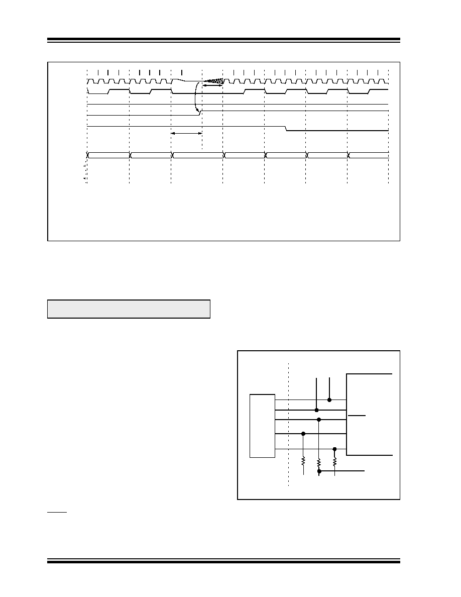
FIGURE 12-14:
WAKE-UP FROM SLEEP THROUGH INTERRUPT
12.9
Program Verification/Code
Protection
If the code protection bit(s) have not been pro-
grammed, the on-chip program memory can be read
out for verification purposes.
12.10 ID Locations
Four memory locations (2000h - 2003h) are designated
as ID locations, where the user can store checksum or
other code identification numbers. These locations are
not accessible during normal execution, but are read-
able and writable during program/verify. It is recom-
mended that only the four Least Significant bits of the
ID location are used.
12.11
In-Circuit Serial Programming
PIC16CXXX microcontrollers can be serially pro-
grammed while in the end application circuit. This is
simply done with two lines for clock and data, and three
other lines for power, ground, and the programming
voltage. This allows customers to manufacture boards
with unprogrammed devices, and then program the
microcontroller just before shipping the product. This
also allows the most recent firmware or a custom firm-
ware to be programmed.
The device is placed into a Program/Verify mode by
holding the RB6 and RB7 pins low, while raising the
MCLR (VPP) pin from VIL to VIHH (see programming
specification). RB6 becomes the programming clock
and RB7 becomes the programming data. Both RB6
and RB7 are Schmitt Trigger inputs in this mode.
After RESET, to place the device into Program/Verify
mode, the program counter (PC) is at location 00h. A
6-bit command is then supplied to the device. Depend-
ing on the command, 14-bits of program data are then
supplied to or from the device, depending if the com-
mand was a load or a read. For complete details of
serial programming, please refer to the PIC16C6X/7X
Programming Specifications (Literature #DS30228).
FIGURE 12-15:
TYPICAL IN-CIRCUIT
SERIAL PROGRAMMING
CONNECTION
Q1 Q2 Q3 Q4 Q1 Q2 Q3 Q4 Q1
Q1 Q2 Q3 Q4 Q1 Q2 Q3 Q4 Q1 Q2 Q3 Q4 Q1 Q2 Q3 Q4
OSC1
CLKOUT(4)
INT pin
INTF Flag
(INTCON<1>)
GIE bit
(INTCON<7>)
INSTRUCTION FLOW
PC
Instruction
Fetched
Instruction
Executed
PC
PC+1
PC+2
Inst(PC) = SLEEP
Inst(PC - 1)
Inst(PC + 1)
SLEEP
Processor in
SLEEP
Interrupt Latency
(Note 2)
Inst(PC + 2)
Inst(PC + 1)
Inst(0004h)
Inst(0005h)
Inst(0004h)
Dummy cycle
PC + 2
0004h
0005h
Dummy cycle
TOST(2)
PC+2
Note
1:
XT, HS or LP oscillator mode assumed.
2:
TOST = 1024TOSC (drawing not to scale) This delay will not be there for RC osc mode.
3:
GIE = ’1’ assumed. In this case after wake-up, the processor jumps to the interrupt routine.
If GIE = ’0’, execution will continue in-line.
4:
CLKOUT is not available in these osc modes, but shown here for timing reference.
Note:
Microchip does not recommend code pro-
tecting windowed devices.
External
Connector
Signals
To Normal
Connections
To Normal
Connections
PIC16CXXX
VDD
VSS
MCLR/VPP
RB6
RB7
+5V
0V
VPP
CLK
Data I/O
VDD
相关PDF资料 |
PDF描述 |
|---|---|
| PIC16F1518-I/SO | 8-BIT, FLASH, RISC MICROCONTROLLER, PDSO28 |
| PIC16F1518T-E/MV | RISC MICROCONTROLLER, PQCC28 |
| PIC16LF1519-E/MV | 8-BIT, FLASH, RISC MICROCONTROLLER, PQCC40 |
| PIC16F1783-E/SO | 8-BIT, FLASH, 32 MHz, RISC MICROCONTROLLER, PDSO28 |
| PIC16F676-E/SL | 8-BIT, FLASH, 20 MHz, RISC MICROCONTROLLER, PDSO14 |
相关代理商/技术参数 |
参数描述 |
|---|---|
| PIC16LC926T-I/L | 功能描述:8位微控制器 -MCU 14KB 336 RAM 52 I/O RoHS:否 制造商:Silicon Labs 核心:8051 处理器系列:C8051F39x 数据总线宽度:8 bit 最大时钟频率:50 MHz 程序存储器大小:16 KB 数据 RAM 大小:1 KB 片上 ADC:Yes 工作电源电压:1.8 V to 3.6 V 工作温度范围:- 40 C to + 105 C 封装 / 箱体:QFN-20 安装风格:SMD/SMT |
| PIC16LC926T-I/PT | 功能描述:8位微控制器 -MCU 14KB 336 RAM 52 I/O RoHS:否 制造商:Silicon Labs 核心:8051 处理器系列:C8051F39x 数据总线宽度:8 bit 最大时钟频率:50 MHz 程序存储器大小:16 KB 数据 RAM 大小:1 KB 片上 ADC:Yes 工作电源电压:1.8 V to 3.6 V 工作温度范围:- 40 C to + 105 C 封装 / 箱体:QFN-20 安装风格:SMD/SMT |
| PIC16LCE623-04/P | 功能描述:8位微控制器 -MCU .875KB 96 RAM 13 I/O RoHS:否 制造商:Silicon Labs 核心:8051 处理器系列:C8051F39x 数据总线宽度:8 bit 最大时钟频率:50 MHz 程序存储器大小:16 KB 数据 RAM 大小:1 KB 片上 ADC:Yes 工作电源电压:1.8 V to 3.6 V 工作温度范围:- 40 C to + 105 C 封装 / 箱体:QFN-20 安装风格:SMD/SMT |
| PIC16LCE623-04/SO | 功能描述:8位微控制器 -MCU .875KB 96 RAM 13 I/O RoHS:否 制造商:Silicon Labs 核心:8051 处理器系列:C8051F39x 数据总线宽度:8 bit 最大时钟频率:50 MHz 程序存储器大小:16 KB 数据 RAM 大小:1 KB 片上 ADC:Yes 工作电源电压:1.8 V to 3.6 V 工作温度范围:- 40 C to + 105 C 封装 / 箱体:QFN-20 安装风格:SMD/SMT |
| PIC16LCE623-04/SS | 功能描述:8位微控制器 -MCU .875KB 96 RAM 13 I/O RoHS:否 制造商:Silicon Labs 核心:8051 处理器系列:C8051F39x 数据总线宽度:8 bit 最大时钟频率:50 MHz 程序存储器大小:16 KB 数据 RAM 大小:1 KB 片上 ADC:Yes 工作电源电压:1.8 V to 3.6 V 工作温度范围:- 40 C to + 105 C 封装 / 箱体:QFN-20 安装风格:SMD/SMT |
发布紧急采购,3分钟左右您将得到回复。