- 您现在的位置:买卖IC网 > PDF目录299771 > PIC16LC926-I/PT 8-BIT, OTPROM, 10 MHz, RISC MICROCONTROLLER, PQFP64 PDF资料下载
参数资料
| 型号: | PIC16LC926-I/PT |
| 元件分类: | 微控制器/微处理器 |
| 英文描述: | 8-BIT, OTPROM, 10 MHz, RISC MICROCONTROLLER, PQFP64 |
| 封装: | 10 X 10 MM, 1 MM HEIGHT, PLASTIC, TQFP-64 |
| 文件页数: | 155/183页 |
| 文件大小: | 3233K |
| 代理商: | PIC16LC926-I/PT |
第1页第2页第3页第4页第5页第6页第7页第8页第9页第10页第11页第12页第13页第14页第15页第16页第17页第18页第19页第20页第21页第22页第23页第24页第25页第26页第27页第28页第29页第30页第31页第32页第33页第34页第35页第36页第37页第38页第39页第40页第41页第42页第43页第44页第45页第46页第47页第48页第49页第50页第51页第52页第53页第54页第55页第56页第57页第58页第59页第60页第61页第62页第63页第64页第65页第66页第67页第68页第69页第70页第71页第72页第73页第74页第75页第76页第77页第78页第79页第80页第81页第82页第83页第84页第85页第86页第87页第88页第89页第90页第91页第92页第93页第94页第95页第96页第97页第98页第99页第100页第101页第102页第103页第104页第105页第106页第107页第108页第109页第110页第111页第112页第113页第114页第115页第116页第117页第118页第119页第120页第121页第122页第123页第124页第125页第126页第127页第128页第129页第130页第131页第132页第133页第134页第135页第136页第137页第138页第139页第140页第141页第142页第143页第144页第145页第146页第147页第148页第149页第150页第151页第152页第153页第154页当前第155页第156页第157页第158页第159页第160页第161页第162页第163页第164页第165页第166页第167页第168页第169页第170页第171页第172页第173页第174页第175页第176页第177页第178页第179页第180页第181页第182页第183页
2001 Microchip Technology Inc.
Preliminary
DS39544A-page 71
PIC16C925/926
9.3.1.2
Reception
When the R/W bit of the address byte is clear and an
address match occurs, the R/W bit of the SSPSTAT
register is cleared. The received address is loaded into
the SSPBUF register.
When the address byte overflow condition exists, then
no Acknowledge (ACK) pulse is given. An overflow
condition is defined as either bit BF (SSPSTAT<0>) is
set, or bit SSPOV (SSPCON<6>) is set.
An SSP interrupt is generated for each data transfer
byte. Flag bit SSPIF (PIR1<3>) must be cleared in soft-
ware. The SSPSTAT register is used to determine the
status of the byte.
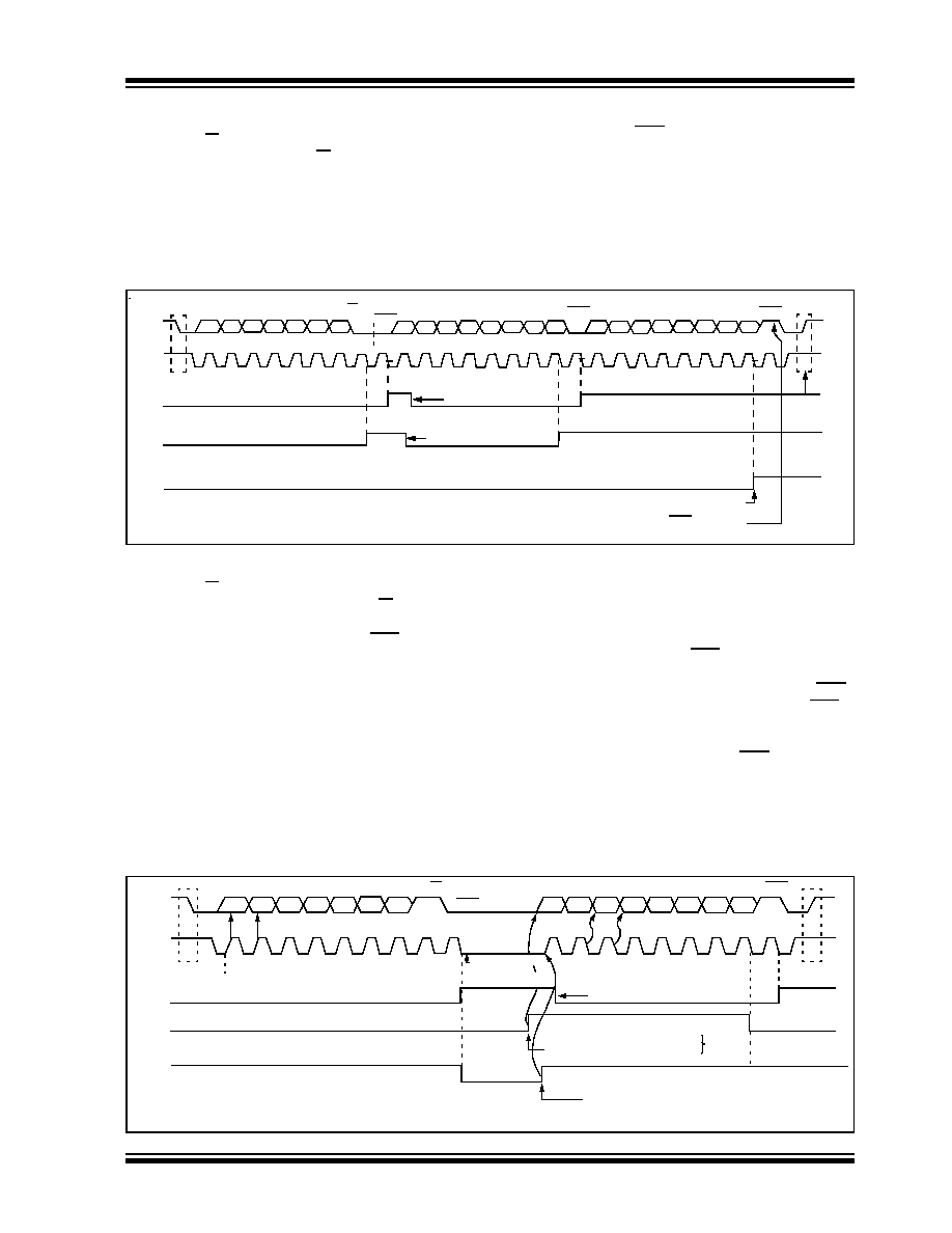
FIGURE 9-17:
I2C WAVEFORMS FOR RECEPTION (7-BIT ADDRESS)
9.3.1.3
Transmission
When the R/W bit of the incoming address byte is set
and an address match occurs, the R/W bit of the
SSPSTAT register is set. The received address is
loaded into the SSPBUF register. The ACK pulse will
be sent on the ninth bit, and pin RC3/SCK/SCL is held
low. The transmit data must be loaded into the
SSPBUF register, which also loads the SSPSR regis-
ter. Then, pin RC3/SCK/SCL should be enabled by set-
ting bit CKP (SSPCON<4>). The master must monitor
the SCL pin prior to asserting another clock pulse. The
slave devices may be holding off the master by stretch-
ing the clock. The eight data bits are shifted out on the
falling edge of the SCL input. This ensures that the
SDA signal is valid during the SCL high time
An SSP interrupt is generated for each data transfer
byte. Flag bit SSPIF must be cleared in software, and
the SSPSTAT register is used to determine the status
of the byte. Flag bit SSPIF is set on the falling edge of
the ninth clock pulse.
As a slave-transmitter, the ACK pulse from the mas-
ter-receiver is latched on the rising edge of the ninth
SCL input pulse. If the SDA line was high (not ACK),
then the data transfer is complete. When the ACK is
latched by the slave, the slave logic is reset and the
slave then monitors for another occurrence of the
START bit. If the SDA line was low (ACK), the transmit
data must be loaded into the SSPBUF register, which
also
loads
the
SSPSR
register.
Then,
pin
RC3/SCK/SCL should be enabled by setting bit CKP.
FIGURE 9-18:
I2C WAVEFORMS FOR TRANSMISSION (7-BIT ADDRESS)
P
9
8
7
6
5
D0
D1
D2
D3
D4
D5
D6
D7
S
A7 A6 A5 A4 A3 A2 A1
SDA
SCL
12
3
4
5
6
7
8
9
12
3
4
56
7
89
12
3
4
Bus Master
terminates
transfer
Bit SSPOV is set because the SSPBUF register is still full.
Cleared in software
SSPBUF register is read
ACK
Receiving Data
D0
D1
D2
D3
D4
D5
D6
D7
ACK
R/W=0
Receiving Address
SSPIF (PIR1<3>)
BF (SSPSTAT<0>)
SSPOV (SSPCON<6>)
ACK
ACK is not sent.
SDA
SCL
SSPIF (PIR1<3>)
BF (SSPSTAT<0>)
CKP (SSPCON<4>)
A7
A6
A5
A4
A3
A2
A1
ACK
D7
D6
D5
D4
D3
D2
D1
D0
ACK
Transmitting Data
R/W = 1
Receiving Address
1
2
3
4
56
789
123
4
5
67
8
9
P
Cleared in software
SSPBUF is written in software
From SSP Interrupt
Service Routine
Set bit after writing to SSPBUF
S
Data in
sampled
SCL held low
while CPU
responds to SSPIF
(the SSPBUF must be written-to
before the CKP bit can be set)
相关PDF资料 |
PDF描述 |
|---|---|
| PIC16F1518-I/SO | 8-BIT, FLASH, RISC MICROCONTROLLER, PDSO28 |
| PIC16F1518T-E/MV | RISC MICROCONTROLLER, PQCC28 |
| PIC16LF1519-E/MV | 8-BIT, FLASH, RISC MICROCONTROLLER, PQCC40 |
| PIC16F1783-E/SO | 8-BIT, FLASH, 32 MHz, RISC MICROCONTROLLER, PDSO28 |
| PIC16F676-E/SL | 8-BIT, FLASH, 20 MHz, RISC MICROCONTROLLER, PDSO14 |
相关代理商/技术参数 |
参数描述 |
|---|---|
| PIC16LC926T-I/L | 功能描述:8位微控制器 -MCU 14KB 336 RAM 52 I/O RoHS:否 制造商:Silicon Labs 核心:8051 处理器系列:C8051F39x 数据总线宽度:8 bit 最大时钟频率:50 MHz 程序存储器大小:16 KB 数据 RAM 大小:1 KB 片上 ADC:Yes 工作电源电压:1.8 V to 3.6 V 工作温度范围:- 40 C to + 105 C 封装 / 箱体:QFN-20 安装风格:SMD/SMT |
| PIC16LC926T-I/PT | 功能描述:8位微控制器 -MCU 14KB 336 RAM 52 I/O RoHS:否 制造商:Silicon Labs 核心:8051 处理器系列:C8051F39x 数据总线宽度:8 bit 最大时钟频率:50 MHz 程序存储器大小:16 KB 数据 RAM 大小:1 KB 片上 ADC:Yes 工作电源电压:1.8 V to 3.6 V 工作温度范围:- 40 C to + 105 C 封装 / 箱体:QFN-20 安装风格:SMD/SMT |
| PIC16LCE623-04/P | 功能描述:8位微控制器 -MCU .875KB 96 RAM 13 I/O RoHS:否 制造商:Silicon Labs 核心:8051 处理器系列:C8051F39x 数据总线宽度:8 bit 最大时钟频率:50 MHz 程序存储器大小:16 KB 数据 RAM 大小:1 KB 片上 ADC:Yes 工作电源电压:1.8 V to 3.6 V 工作温度范围:- 40 C to + 105 C 封装 / 箱体:QFN-20 安装风格:SMD/SMT |
| PIC16LCE623-04/SO | 功能描述:8位微控制器 -MCU .875KB 96 RAM 13 I/O RoHS:否 制造商:Silicon Labs 核心:8051 处理器系列:C8051F39x 数据总线宽度:8 bit 最大时钟频率:50 MHz 程序存储器大小:16 KB 数据 RAM 大小:1 KB 片上 ADC:Yes 工作电源电压:1.8 V to 3.6 V 工作温度范围:- 40 C to + 105 C 封装 / 箱体:QFN-20 安装风格:SMD/SMT |
| PIC16LCE623-04/SS | 功能描述:8位微控制器 -MCU .875KB 96 RAM 13 I/O RoHS:否 制造商:Silicon Labs 核心:8051 处理器系列:C8051F39x 数据总线宽度:8 bit 最大时钟频率:50 MHz 程序存储器大小:16 KB 数据 RAM 大小:1 KB 片上 ADC:Yes 工作电源电压:1.8 V to 3.6 V 工作温度范围:- 40 C to + 105 C 封装 / 箱体:QFN-20 安装风格:SMD/SMT |
发布紧急采购,3分钟左右您将得到回复。