- 您现在的位置:买卖IC网 > PDF目录299771 > PIC16LC926-I/PT 8-BIT, OTPROM, 10 MHz, RISC MICROCONTROLLER, PQFP64 PDF资料下载
参数资料
| 型号: | PIC16LC926-I/PT |
| 元件分类: | 微控制器/微处理器 |
| 英文描述: | 8-BIT, OTPROM, 10 MHz, RISC MICROCONTROLLER, PQFP64 |
| 封装: | 10 X 10 MM, 1 MM HEIGHT, PLASTIC, TQFP-64 |
| 文件页数: | 165/183页 |
| 文件大小: | 3233K |
| 代理商: | PIC16LC926-I/PT |
第1页第2页第3页第4页第5页第6页第7页第8页第9页第10页第11页第12页第13页第14页第15页第16页第17页第18页第19页第20页第21页第22页第23页第24页第25页第26页第27页第28页第29页第30页第31页第32页第33页第34页第35页第36页第37页第38页第39页第40页第41页第42页第43页第44页第45页第46页第47页第48页第49页第50页第51页第52页第53页第54页第55页第56页第57页第58页第59页第60页第61页第62页第63页第64页第65页第66页第67页第68页第69页第70页第71页第72页第73页第74页第75页第76页第77页第78页第79页第80页第81页第82页第83页第84页第85页第86页第87页第88页第89页第90页第91页第92页第93页第94页第95页第96页第97页第98页第99页第100页第101页第102页第103页第104页第105页第106页第107页第108页第109页第110页第111页第112页第113页第114页第115页第116页第117页第118页第119页第120页第121页第122页第123页第124页第125页第126页第127页第128页第129页第130页第131页第132页第133页第134页第135页第136页第137页第138页第139页第140页第141页第142页第143页第144页第145页第146页第147页第148页第149页第150页第151页第152页第153页第154页第155页第156页第157页第158页第159页第160页第161页第162页第163页第164页当前第165页第166页第167页第168页第169页第170页第171页第172页第173页第174页第175页第176页第177页第178页第179页第180页第181页第182页第183页
PIC16C925/926
DS39544A-page 80
Preliminary
2001 Microchip Technology Inc.
10.3
Configuring Analog Port Pins
The ADCON1 and TRIS registers control the operation
of the A/D port pins. The port pins that are desired as
analog inputs must have their corresponding TRIS bits
set (input). If the TRIS bit is cleared (output), the digital
output level (VOH or VOL) will be converted.
The A/D operation is independent of the state of the
CHS<2:0> bits and the TRIS bits.
10.4
A/D Conversions
Clearing the GO/DONE bit during a conversion will
abort the current conversion. The A/D result register
pair will NOT be updated with the partially completed
A/D conversion sample. That is, the ADRESH:ADRESL
registers will continue to contain the value of the last
completed conversion (or the last value written to the
ADRESH:ADRESL registers). After the A/D conversion
is aborted, a 2TAD wait is required before the next
acquisition is started. After this 2TAD wait, acquisition
on the selected channel is automatically started. After
this, the GO/DONE bit can be set to start the
conversion.
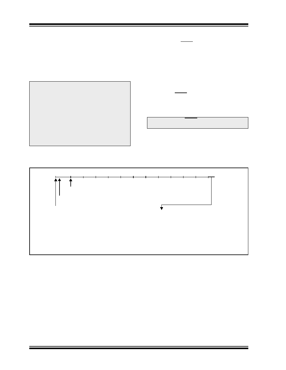
In Figure 10-3, after the GO bit is set, the first time seg-
ment has a minimum of TCY and a maximum of TAD.
FIGURE 10-3:
A/D CONVERSION TAD CYCLES
10.4.1
A/D RESULT REGISTERS
The ADRESH:ADRESL register pair is the location
where the 10-bit A/D result is loaded at the completion
of the A/D conversion. This register pair is 16-bits wide.
The A/D module gives the flexibility to left or right justify
the 10-bit result in the 16-bit result register. The A/D
Format Select bit (ADFM) controls this justification.
Figure 10-4 shows the operation of the A/D result justi-
fication. The extra bits are loaded with ’0’s’. When an
A/D result will not overwrite these locations (A/D dis-
able), these registers may be used as two general pur-
pose 8-bit registers.
Note 1: When reading the port register, any pin
configured as an analog input channel will
read as cleared (a low level). Pins config-
ured as digital inputs will convert an ana-
log input. Analog levels on a digitally
configured input will not affect the conver-
sion accuracy.
2: Analog levels on any pin that is defined as
a digital input (including the AN<4:0>
pins), may cause the input buffer to con-
sume current that is out of the device
specifications.
Note:
The GO/DONE bit should NOT be set in
the same instruction that turns on the A/D.
TAD1
TAD2
TAD3
TAD4
TAD5
TAD6
TAD7
TAD8
TAD9
Set GO bit
Holding capacitor is disconnected from analog input (typically 100 ns)
b9
b8
b7
b6
b5
b4
b3
b2
TAD10 TAD11
b1
b0
TCY to TAD
Conversion Starts
ADRES is loaded,
GO bit is cleared,
ADIF bit is set,
holding capacitor is connected to analog input.
A 2TAD wait is necessary before the next
acquisition is started.
相关PDF资料 |
PDF描述 |
|---|---|
| PIC16F1518-I/SO | 8-BIT, FLASH, RISC MICROCONTROLLER, PDSO28 |
| PIC16F1518T-E/MV | RISC MICROCONTROLLER, PQCC28 |
| PIC16LF1519-E/MV | 8-BIT, FLASH, RISC MICROCONTROLLER, PQCC40 |
| PIC16F1783-E/SO | 8-BIT, FLASH, 32 MHz, RISC MICROCONTROLLER, PDSO28 |
| PIC16F676-E/SL | 8-BIT, FLASH, 20 MHz, RISC MICROCONTROLLER, PDSO14 |
相关代理商/技术参数 |
参数描述 |
|---|---|
| PIC16LC926T-I/L | 功能描述:8位微控制器 -MCU 14KB 336 RAM 52 I/O RoHS:否 制造商:Silicon Labs 核心:8051 处理器系列:C8051F39x 数据总线宽度:8 bit 最大时钟频率:50 MHz 程序存储器大小:16 KB 数据 RAM 大小:1 KB 片上 ADC:Yes 工作电源电压:1.8 V to 3.6 V 工作温度范围:- 40 C to + 105 C 封装 / 箱体:QFN-20 安装风格:SMD/SMT |
| PIC16LC926T-I/PT | 功能描述:8位微控制器 -MCU 14KB 336 RAM 52 I/O RoHS:否 制造商:Silicon Labs 核心:8051 处理器系列:C8051F39x 数据总线宽度:8 bit 最大时钟频率:50 MHz 程序存储器大小:16 KB 数据 RAM 大小:1 KB 片上 ADC:Yes 工作电源电压:1.8 V to 3.6 V 工作温度范围:- 40 C to + 105 C 封装 / 箱体:QFN-20 安装风格:SMD/SMT |
| PIC16LCE623-04/P | 功能描述:8位微控制器 -MCU .875KB 96 RAM 13 I/O RoHS:否 制造商:Silicon Labs 核心:8051 处理器系列:C8051F39x 数据总线宽度:8 bit 最大时钟频率:50 MHz 程序存储器大小:16 KB 数据 RAM 大小:1 KB 片上 ADC:Yes 工作电源电压:1.8 V to 3.6 V 工作温度范围:- 40 C to + 105 C 封装 / 箱体:QFN-20 安装风格:SMD/SMT |
| PIC16LCE623-04/SO | 功能描述:8位微控制器 -MCU .875KB 96 RAM 13 I/O RoHS:否 制造商:Silicon Labs 核心:8051 处理器系列:C8051F39x 数据总线宽度:8 bit 最大时钟频率:50 MHz 程序存储器大小:16 KB 数据 RAM 大小:1 KB 片上 ADC:Yes 工作电源电压:1.8 V to 3.6 V 工作温度范围:- 40 C to + 105 C 封装 / 箱体:QFN-20 安装风格:SMD/SMT |
| PIC16LCE623-04/SS | 功能描述:8位微控制器 -MCU .875KB 96 RAM 13 I/O RoHS:否 制造商:Silicon Labs 核心:8051 处理器系列:C8051F39x 数据总线宽度:8 bit 最大时钟频率:50 MHz 程序存储器大小:16 KB 数据 RAM 大小:1 KB 片上 ADC:Yes 工作电源电压:1.8 V to 3.6 V 工作温度范围:- 40 C to + 105 C 封装 / 箱体:QFN-20 安装风格:SMD/SMT |
发布紧急采购,3分钟左右您将得到回复。