- 您现在的位置:买卖IC网 > PDF目录299771 > PIC16LF818T-I/SS 8-BIT, FLASH, 10 MHz, RISC MICROCONTROLLER, PDSO20 PDF资料下载
参数资料
| 型号: | PIC16LF818T-I/SS |
| 元件分类: | 微控制器/微处理器 |
| 英文描述: | 8-BIT, FLASH, 10 MHz, RISC MICROCONTROLLER, PDSO20 |
| 封装: | 0.209 INCH, PLASTIC, MO-150, SSOP-20 |
| 文件页数: | 161/176页 |
| 文件大小: | 3124K |
| 代理商: | PIC16LF818T-I/SS |
第1页第2页第3页第4页第5页第6页第7页第8页第9页第10页第11页第12页第13页第14页第15页第16页第17页第18页第19页第20页第21页第22页第23页第24页第25页第26页第27页第28页第29页第30页第31页第32页第33页第34页第35页第36页第37页第38页第39页第40页第41页第42页第43页第44页第45页第46页第47页第48页第49页第50页第51页第52页第53页第54页第55页第56页第57页第58页第59页第60页第61页第62页第63页第64页第65页第66页第67页第68页第69页第70页第71页第72页第73页第74页第75页第76页第77页第78页第79页第80页第81页第82页第83页第84页第85页第86页第87页第88页第89页第90页第91页第92页第93页第94页第95页第96页第97页第98页第99页第100页第101页第102页第103页第104页第105页第106页第107页第108页第109页第110页第111页第112页第113页第114页第115页第116页第117页第118页第119页第120页第121页第122页第123页第124页第125页第126页第127页第128页第129页第130页第131页第132页第133页第134页第135页第136页第137页第138页第139页第140页第141页第142页第143页第144页第145页第146页第147页第148页第149页第150页第151页第152页第153页第154页第155页第156页第157页第158页第159页第160页当前第161页第162页第163页第164页第165页第166页第167页第168页第169页第170页第171页第172页第173页第174页第175页第176页
2003 Microchip Technology Inc.
DS39598D-page 83
PIC16F818/819
The ADRESH:ADRESL registers contain the result of
the A/D conversion. When the A/D conversion is
complete, the result is loaded into the A/D Result register
pair, the GO/DONE bit (ADCON0<2>) is cleared and
A/D Interrupt Flag bit, ADIF, is set. The block diagram of
the A/D module is shown in Figure 11-1.
After the A/D module has been configured as desired,
the selected channel must be acquired before the
conversion is started. The analog input channels must
have their corresponding TRIS bits selected as inputs.
To determine sample time, see Section 11.1 “A/D
Acquisition Requirements”. After this sample time
has elapsed, the A/D conversion can be started.
These steps should be followed for doing an A/D
conversion:
1.
Configure the A/D module:
Configure analog pins/voltage reference and
digital I/O (ADCON1)
Select A/D input channel (ADCON0)
Select A/D conversion clock (ADCON0)
Turn on A/D module (ADCON0)
2.
Configure A/D interrupt (if desired):
Clear ADIF bit
Set ADIE bit
Set GIE bit
3.
Wait the required acquisition time.
4.
Start conversion:
Set GO/DONE bit (ADCON0)
5.
Wait for A/D conversion to complete by either:
Polling for the GO/DONE bit to be cleared
(with interrupts disabled); OR
Waiting for the A/D interrupt
6.
Read A/D Result register pair
(ADRESH:ADRESL), clear bit ADIF if required.
7.
For next conversion, go to step 1 or step 2 as
required. The A/D conversion time per bit is
defined as TAD. A minimum wait of 2 TAD is
required before the next acquisition starts.
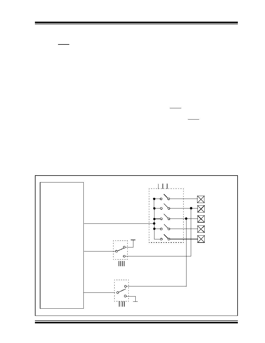
FIGURE 11-1:
A/D BLOCK DIAGRAM
(Input Voltage)
VIN
VREF+
(Reference
Voltage)
AVDD
PCFG<3:0>
CHS<3:0>
RA3/AN3/VREF+
RA2/AN2/VREF-
RA1/AN1
RA0/AN0
011
010
001
000
A/D
Converter
VREF-
(Reference
Voltage)
AVSS
PCFG<3:0>
RA4/AN4/T0CKI
100
相关PDF资料 |
PDF描述 |
|---|---|
| PIC16LF877T-20/PT | 8-BIT, FLASH, 20 MHz, RISC MICROCONTROLLER, PQFP44 |
| PIC18F242T-I/SO | 8-BIT, FLASH, 40 MHz, RISC MICROCONTROLLER, PDSO28 |
| PIC18F442-E/L | 8-BIT, FLASH, 40 MHz, RISC MICROCONTROLLER, PQCC44 |
| PIC18F258I/SP | 8-BIT, FLASH, 40 MHz, RISC MICROCONTROLLER, PDIP28 |
| PIC18LF448-I/PT | 8-BIT, FLASH, 40 MHz, RISC MICROCONTROLLER, PQFP44 |
相关代理商/技术参数 |
参数描述 |
|---|---|
| PIC16LF819-I/ML | 功能描述:8位微控制器 -MCU 3.5KB 256 RAM 16 I/O RoHS:否 制造商:Silicon Labs 核心:8051 处理器系列:C8051F39x 数据总线宽度:8 bit 最大时钟频率:50 MHz 程序存储器大小:16 KB 数据 RAM 大小:1 KB 片上 ADC:Yes 工作电源电压:1.8 V to 3.6 V 工作温度范围:- 40 C to + 105 C 封装 / 箱体:QFN-20 安装风格:SMD/SMT |
| PIC16LF819-I/MLTSL | 功能描述:8位微控制器 -MCU 3.5 KB FL 256 RAM 16 I/O RoHS:否 制造商:Silicon Labs 核心:8051 处理器系列:C8051F39x 数据总线宽度:8 bit 最大时钟频率:50 MHz 程序存储器大小:16 KB 数据 RAM 大小:1 KB 片上 ADC:Yes 工作电源电压:1.8 V to 3.6 V 工作温度范围:- 40 C to + 105 C 封装 / 箱体:QFN-20 安装风格:SMD/SMT |
| PIC16LF819-I/P | 功能描述:8位微控制器 -MCU 3.5KB 256 RAM 16 I/O RoHS:否 制造商:Silicon Labs 核心:8051 处理器系列:C8051F39x 数据总线宽度:8 bit 最大时钟频率:50 MHz 程序存储器大小:16 KB 数据 RAM 大小:1 KB 片上 ADC:Yes 工作电源电压:1.8 V to 3.6 V 工作温度范围:- 40 C to + 105 C 封装 / 箱体:QFN-20 安装风格:SMD/SMT |
| PIC16LF819-I/PTSL | 功能描述:8位微控制器 -MCU 3.5 KB FL 256 RAM 16 I/O RoHS:否 制造商:Silicon Labs 核心:8051 处理器系列:C8051F39x 数据总线宽度:8 bit 最大时钟频率:50 MHz 程序存储器大小:16 KB 数据 RAM 大小:1 KB 片上 ADC:Yes 工作电源电压:1.8 V to 3.6 V 工作温度范围:- 40 C to + 105 C 封装 / 箱体:QFN-20 安装风格:SMD/SMT |
| PIC16LF819-I/SO | 功能描述:8位微控制器 -MCU 3.5KB 256 RAM 16 I/O RoHS:否 制造商:Silicon Labs 核心:8051 处理器系列:C8051F39x 数据总线宽度:8 bit 最大时钟频率:50 MHz 程序存储器大小:16 KB 数据 RAM 大小:1 KB 片上 ADC:Yes 工作电源电压:1.8 V to 3.6 V 工作温度范围:- 40 C to + 105 C 封装 / 箱体:QFN-20 安装风格:SMD/SMT |
发布紧急采购,3分钟左右您将得到回复。