- 您现在的位置:买卖IC网 > PDF目录296863 > PSD913F1V-12B81I (意法半导体) Flash In-System Programmable ISP Peripherals For 8-bit MCUs PDF资料下载
参数资料
| 型号: | PSD913F1V-12B81I |
| 厂商: | 意法半导体 |
| 英文描述: | Flash In-System Programmable ISP Peripherals For 8-bit MCUs |
| 中文描述: | Flash在系统可编程ISP的外设的8位微控制器 |
| 文件页数: | 7/94页 |
| 文件大小: | 476K |
| 代理商: | PSD913F1V-12B81I |
第1页第2页第3页第4页第5页第6页当前第7页第8页第9页第10页第11页第12页第13页第14页第15页第16页第17页第18页第19页第20页第21页第22页第23页第24页第25页第26页第27页第28页第29页第30页第31页第32页第33页第34页第35页第36页第37页第38页第39页第40页第41页第42页第43页第44页第45页第46页第47页第48页第49页第50页第51页第52页第53页第54页第55页第56页第57页第58页第59页第60页第61页第62页第63页第64页第65页第66页第67页第68页第69页第70页第71页第72页第73页第74页第75页第76页第77页第78页第79页第80页第81页第82页第83页第84页第85页第86页第87页第88页第89页第90页第91页第92页第93页第94页
Preliminary Information
PSD9XX Family
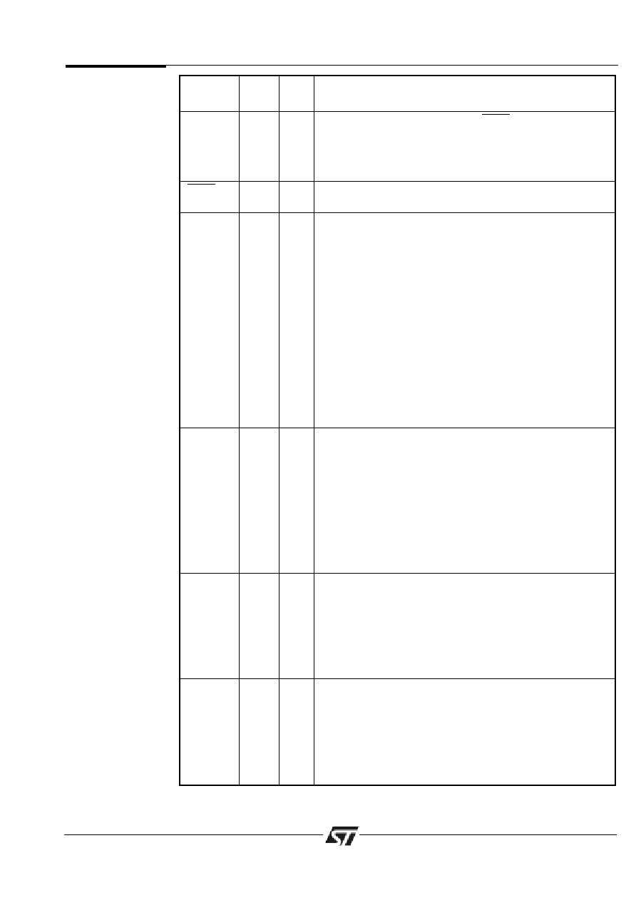
Pin Name Pin*
Type
Description
(PLCC)
CNTL2
49
I
This pin can be used to input the PSEN (Program Select
Enable) signal from any MCU that uses this signal for code
exclusively. If your MCU does not output a Program Select
Enable signal, this port can be used as a generic input. This
port is connected to the PLDs.
Reset
48
I
Active low reset input. Resets I/O Ports and some of the
configuration registers. Must be active at power up.
PA0
29
I/O
These pins make up Port A. These port pins are configurable
PA1
28
and can have the following functions:
PA2
27
1. MCU I/O — write to or read from a standard output or
PA3
25
input port.
PA4
24
2. General Purpose PLD outputs.
PA5
23
3. Inputs to the PLDs.
PA6
22
4. Latched address outputs (see Table 6).
PA7
21
5. Address inputs. For example, PA0-3 could be used for
A[0:3] when using an 80C51XA in burst mode.
6. As the data bus inputs D[0:7] for non-multiplexed
address/data bus MCUs.
7. D0/A16-D3/A19 in M37702M2 mode.
Note: PA0-3 can only output CMOS signals with an option
for high slew rate. However, PA4-7 can be configured as
CMOS or Open Drain Outputs.
PB0
7
I/O
These pins make up Port B. These port pins are configurable
PB1
6
and can have the following functions:
PB2
5
1. MCU I/O — write to or read from a standard output or
PB3
4
input port.
PB4
3
2. General Purpose PLD outputs.
PB5
2
3. Inputs to the PLDs.
PB6
52
4. Latched address outputs (see Table 6).
PB7
51
Note: PB0-3 can only output CMOS signals with an option
for high slew rate. However, PB4-7 can be configured as
CMOS or Open Drain Outputs.
PC0
20
I/O
PC0 pin of Port C. This port pin can be configured to have
the following functions:
1. MCU I/O — write to or read from a standard output or
input port.
2. Input to the PLDs.
3. TMS Input for the JTAG Interface.
This pin can be configured as a CMOS or Open Drain output.
PC1
19
I/O
PC1 pin of Port C. This port pin can be configured to have
the following functions:
1. MCU I/O — write to or read from a standard output or
input port.
2. Input to the PLDs.
3. TCK Input for the JTAG Interface.
This pin can be configured as a CMOS or Open Drain output.
Table 5.
PSD9XX
Pin
Descriptions
(cont.)
11
相关PDF资料 |
PDF描述 |
|---|---|
| PSD913F1V-12J | Flash In-System Programmable ISP Peripherals For 8-bit MCUs |
| PSD913F1V-12JI | Flash In-System Programmable ISP Peripherals For 8-bit MCUs |
| PSD913F1V-12M | Flash In-System Programmable ISP Peripherals For 8-bit MCUs |
| PSD933212JIT | Flash In-System Programmable ISP Peripherals For 8-bit MCUs |
| PSD933212JT | Flash In-System Programmable ISP Peripherals For 8-bit MCUs |
相关代理商/技术参数 |
参数描述 |
|---|---|
| PSD913F1V-12J | 制造商:STMICROELECTRONICS 制造商全称:STMicroelectronics 功能描述:Flash In-System Programmable ISP Peripherals For 8-bit MCUs |
| PSD913F1V-12JI | 制造商:STMICROELECTRONICS 制造商全称:STMicroelectronics 功能描述:Flash In-System Programmable ISP Peripherals For 8-bit MCUs |
| PSD913F1V-12M | 制造商:STMICROELECTRONICS 制造商全称:STMicroelectronics 功能描述:Flash In-System Programmable ISP Peripherals For 8-bit MCUs |
| PSD913F1V-12MI | 制造商:STMICROELECTRONICS 制造商全称:STMicroelectronics 功能描述:Flash In-System Programmable ISP Peripherals For 8-bit MCUs |
| PSD913F1V-12U | 制造商:STMICROELECTRONICS 制造商全称:STMicroelectronics 功能描述:Flash In-System Programmable ISP Peripherals For 8-bit MCUs |
发布紧急采购,3分钟左右您将得到回复。