- 您现在的位置:买卖IC网 > PDF目录69310 > R5F2138CFJFP FLASH, 20 MHz, MICROCONTROLLER, PQFP80 PDF资料下载
参数资料
| 型号: | R5F2138CFJFP |
| 元件分类: | 微控制器/微处理器 |
| 英文描述: | FLASH, 20 MHz, MICROCONTROLLER, PQFP80 |
| 封装: | 12 X 12 MM, 0.50 MM PITCH, PLASTIC, LQFP-80 |
| 文件页数: | 3/30页 |
| 文件大小: | 483K |
| 代理商: | R5F2138CFJFP |
第1页第2页当前第3页第4页第5页第6页第7页第8页第9页第10页第11页第12页第13页第14页第15页第16页第17页第18页第19页第20页第21页第22页第23页第24页第25页第26页第27页第28页第29页第30页
61
ATmega165A/PA/325A/PA/3250A/PA/645A/P/6450A/P [DATASHEET]
8285E–AVR–02/2013
14. I/O-Ports
14.1
Overview
All AVR ports have true Read-Modify-Write functionality when used as general digital I/O ports. This means that
the direction of one port pin can be changed without unintentionally changing the direction of any other pin with the
SBI and CBI instructions. The same applies when changing drive value (if configured as output) or enabling/dis-
abling of pull-up resistors (if configured as input). Each output buffer has symmetrical drive characteristics with
both high sink and source capability. The pin driver is strong enough to drive LED displays directly. All port pins
have individually selectable pull-up resistors with a supply-voltage invariant resistance. All I/O pins have protection
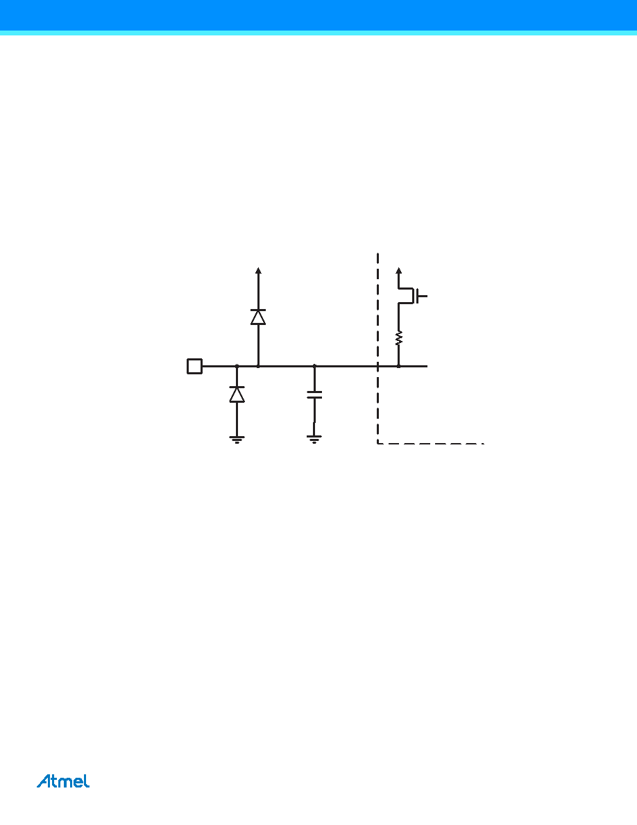
diodes to both V
CC and Ground as indicated in Figure 14-1 on page 61. Refer to ”Electrical characteristics – TA = -
40°C to 85°C” on page 288 for a complete list of parameters. If exceeding the pin voltage “Absolute Maximum Rat-
ings”, resulting currents can harm the device if not limited accordingly.
Figure 14-1. I/O pin equivalent schematic.
All registers and bit references in this section are written in general form. A lower case “x” represents the number-
ing letter for the port, and a lower case “n” represents the bit number. However, when using the register or bit
defines in a program, the precise form must be used. For example, PORTB3 for bit no. 3 in Port B, here docu-
mented generally as PORTxn. The physical I/O Registers and bit locations are listed in ”Register description” on
Three I/O memory address locations are allocated for each port, one each for the Data Register – PORTx, Data
Direction Register – DDRx, and the Port Input Pins – PINx. The Port Input Pins I/O location is read only, while the
Data Register and the Data Direction Register are read/write. However, writing a logic one to a bit in the PINx Reg-
ister, will result in a toggle in the corresponding bit in the Data Register. In addition, the Pull-up Disable – PUD bit
in MCUCR disables the pull-up function for all pins in all ports when set.
Using the I/O port as General Digital I/O is described in ”Ports as general digital I/O” on page 61. Most port pins are
multiplexed with alternate functions for the peripheral features on the device. How each alternate function inter-
feres with the port pin is described in ”Alternate port functions” on page 65. Refer to the individual module sections
for a full description of the alternate functions.
Note that enabling the alternate function of some of the port pins does not affect the use of the other pins in the port
as general digital I/O.
14.2
Ports as general digital I/O
The ports are bi-directional I/O ports with optional internal pull-ups. Figure 14-2 on page 62 shows a functional
description of one I/O-port pin, here generically called Pxn.
C
pin
Logic
R
pu
See Figure
"General Digital I/O" for
Details
Pxn
相关PDF资料 |
PDF描述 |
|---|---|
| R5F2138CHJFP | FLASH, 20 MHz, MICROCONTROLLER, PQFP80 |
| R5F2138AFJFP | FLASH, 20 MHz, MICROCONTROLLER, PQFP80 |
| R5F2138CCNFP | 8-BIT, FLASH, 20 MHz, MICROCONTROLLER, PQFP80 |
| R5F21386CNFP | 8-BIT, FLASH, 20 MHz, MICROCONTROLLER, PQFP80 |
| R5F213G1DDSP | 8-BIT, FLASH, 20 MHz, MICROCONTROLLER, PDSO24 |
相关代理商/技术参数 |
参数描述 |
|---|---|
| R5F2138CMDFD | 制造商:RENESAS 制造商全称:Renesas Technology Corp 功能描述:The R8C/38M Group has data flash (1 KB × 4 blocks) with the background operation |
| R5F2138CMDFP | 制造商:RENESAS 制造商全称:Renesas Technology Corp 功能描述:The R8C/38M Group has data flash (1 KB × 4 blocks) with the background operation |
| R5F2138CMDFP#30 | 制造商:Renesas Electronics Corporation 功能描述:IC MCU 16BIT 128KB FLASH 80LQFP |
| R5F2138CMDFP#V0 | 制造商:Renesas Electronics Corporation 功能描述:IC MCU 16BIT 128KB FLASH 80LQFP |
| R5F2138CMDXXXFD | 制造商:RENESAS 制造商全称:Renesas Technology Corp 功能描述:The R8C/38M Group has data flash (1 KB × 4 blocks) with the background operation |
发布紧急采购,3分钟左右您将得到回复。