- 您现在的位置:买卖IC网 > PDF目录69310 > R5F2138CFJFP FLASH, 20 MHz, MICROCONTROLLER, PQFP80 PDF资料下载
参数资料
| 型号: | R5F2138CFJFP |
| 元件分类: | 微控制器/微处理器 |
| 英文描述: | FLASH, 20 MHz, MICROCONTROLLER, PQFP80 |
| 封装: | 12 X 12 MM, 0.50 MM PITCH, PLASTIC, LQFP-80 |
| 文件页数: | 5/30页 |
| 文件大小: | 483K |
| 代理商: | R5F2138CFJFP |
第1页第2页第3页第4页当前第5页第6页第7页第8页第9页第10页第11页第12页第13页第14页第15页第16页第17页第18页第19页第20页第21页第22页第23页第24页第25页第26页第27页第28页第29页第30页
63
ATmega165A/PA/325A/PA/3250A/PA/645A/P/6450A/P [DATASHEET]
8285E–AVR–02/2013
Switching between input with pull-up and output low generates the same problem. The user must use either the tri-
state ({DDxn, PORTxn} = 0b00) or the output high state ({DDxn, PORTxn} = 0b11) as an intermediate step.
Table 14-1 on page 63 summarizes the control signals for the pin value.
14.2.4
Reading the pin value
Independent of the setting of Data Direction bit DDxn, the port pin can be read through the PINxn Register bit. As
shown in Figure 14-2, the PINxn Register bit and the preceding latch constitute a synchronizer. This is needed to
avoid metastability if the physical pin changes value near the edge of the internal clock, but it also introduces a
delay. Figure 14-3 shows a timing diagram of the synchronization when reading an externally applied pin value.
The maximum and minimum propagation delays are denoted t
pd,max and tpd,min respectively.
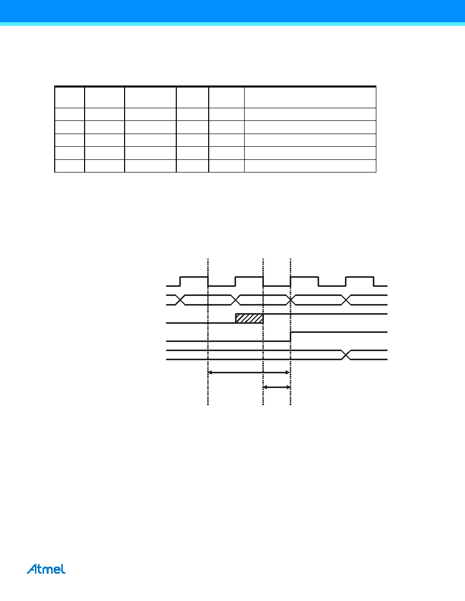
Figure 14-3. Synchronization when reading an externally applied pin value.
Consider the clock period starting shortly after the first falling edge of the system clock. The latch is closed when
the clock is low, and goes transparent when the clock is high, as indicated by the shaded region of the “SYNC
LATCH” signal. The signal value is latched when the system clock goes low. It is clocked into the PINxn Register at
the succeeding positive clock edge. As indicated by the two arrows tpd,max and tpd,min, a single signal transition
on the pin will be delayed between and 1 system clock period depending upon the time of assertion.
When reading back a software assigned pin value, a nop instruction must be inserted as indicated in Figure 14-4
on page 64. The out instruction sets the “SYNC LATCH” signal at the positive edge of the clock. In this case, the
delay tpd through the synchronizer is one system clock period.
Table 14-1.
Port pin configurations.
DDxn
PORTxn
PUD
(in MCUCR)
I/O
Pull-up
Comment
0
X
Input
No
Tri-state (Hi-Z)
0
1
0
Input
Yes
Pxn will source current if ext. pulled low.
0
1
Input
No
Tri-state (Hi-Z)
1
0
X
Output
No
Output Low (Sink)
1
X
Output
No
Output High (Source)
XXX
in r17, PINx
0x00
0xFF
INSTRUCTIONS
SYNC LATCH
PINxn
r17
XXX
SYSTEM CLK
t
pd, max
t pd, min
相关PDF资料 |
PDF描述 |
|---|---|
| R5F2138CHJFP | FLASH, 20 MHz, MICROCONTROLLER, PQFP80 |
| R5F2138AFJFP | FLASH, 20 MHz, MICROCONTROLLER, PQFP80 |
| R5F2138CCNFP | 8-BIT, FLASH, 20 MHz, MICROCONTROLLER, PQFP80 |
| R5F21386CNFP | 8-BIT, FLASH, 20 MHz, MICROCONTROLLER, PQFP80 |
| R5F213G1DDSP | 8-BIT, FLASH, 20 MHz, MICROCONTROLLER, PDSO24 |
相关代理商/技术参数 |
参数描述 |
|---|---|
| R5F2138CMDFD | 制造商:RENESAS 制造商全称:Renesas Technology Corp 功能描述:The R8C/38M Group has data flash (1 KB × 4 blocks) with the background operation |
| R5F2138CMDFP | 制造商:RENESAS 制造商全称:Renesas Technology Corp 功能描述:The R8C/38M Group has data flash (1 KB × 4 blocks) with the background operation |
| R5F2138CMDFP#30 | 制造商:Renesas Electronics Corporation 功能描述:IC MCU 16BIT 128KB FLASH 80LQFP |
| R5F2138CMDFP#V0 | 制造商:Renesas Electronics Corporation 功能描述:IC MCU 16BIT 128KB FLASH 80LQFP |
| R5F2138CMDXXXFD | 制造商:RENESAS 制造商全称:Renesas Technology Corp 功能描述:The R8C/38M Group has data flash (1 KB × 4 blocks) with the background operation |
发布紧急采购,3分钟左右您将得到回复。