- 您现在的位置:买卖IC网 > PDF目录69312 > R5F2L3ACCNFP 8-BIT, FLASH, 20 MHz, MICROCONTROLLER, PQFP100 PDF资料下载
参数资料
| 型号: | R5F2L3ACCNFP |
| 元件分类: | 微控制器/微处理器 |
| 英文描述: | 8-BIT, FLASH, 20 MHz, MICROCONTROLLER, PQFP100 |
| 封装: | 14 X 14 MM, 0.50 MM PITCH, PLASTIC, LQFP-100 |
| 文件页数: | 29/74页 |
| 文件大小: | 959K |
| 代理商: | R5F2L3ACCNFP |
第1页第2页第3页第4页第5页第6页第7页第8页第9页第10页第11页第12页第13页第14页第15页第16页第17页第18页第19页第20页第21页第22页第23页第24页第25页第26页第27页第28页当前第29页第30页第31页第32页第33页第34页第35页第36页第37页第38页第39页第40页第41页第42页第43页第44页第45页第46页第47页第48页第49页第50页第51页第52页第53页第54页第55页第56页第57页第58页第59页第60页第61页第62页第63页第64页第65页第66页第67页第68页第69页第70页第71页第72页第73页第74页
36
2588F–AVR–06/2013
ATtiny261/461/861
7.
Power Management and Sleep Modes
The high performance and industry leading code efficiency makes the AVR microcontrollers an
ideal choise for low power applications. In addition, sleep modes enable the application to shut
down unused modules in the MCU, thereby saving power. The AVR provides various sleep
modes allowing the user to tailor the power consumption to the application’s requirements.
7.1
Sleep Modes
Figure 6-1 on page 24 presents the different clock systems and their distribution in
ATtiny261/461/861. The figure is helpful in selecting an appropriate sleep mode. Table 7-1
shows the different sleep modes and their wake up sources.
Note:
1. For INT0 and INT1, only level interrupt.
2. When PLL selected as system clock.
To enter any of the sleep modes, the SE bit in MCUCR must be written to logic one and a
SLEEP instruction must be executed. The SM1:0 bits in the MCUCR Register select which sleep
mode (Idle, ADC Noise Reduction, Power-down, or Standby) will be activated by the SLEEP
instruction. See Table 7-2 for a summary.
If an enabled interrupt occurs while the MCU is in a sleep mode, the MCU wakes up. The MCU
is then halted for four cycles in addition to the start-up time, executes the interrupt routine, and
resumes execution from the instruction following SLEEP. The contents of the Register File and
SRAM are unaltered when the device wakes up from sleep. If a reset occurs during sleep mode,
the MCU wakes up and executes from the Reset Vector.
Note that if a level triggered interrupt is used for wake-up the changed level must be held for
some time to wake up the MCU (and for the MCU to enter the interrupt service routine). See
“External Interrupts” on page 51 for details.
7.1.1
Idle Mode
When bits SM1:0 are written to 00, the SLEEP instruction makes the MCU enter Idle mode,
stopping the CPU but allowing Analog Comparator, ADC, Timer/Counter, Watchdog, and the
interrupt system to continue operating. This sleep mode basically halts clk
CPU and clkFLASH, while
allowing the other clocks to run.
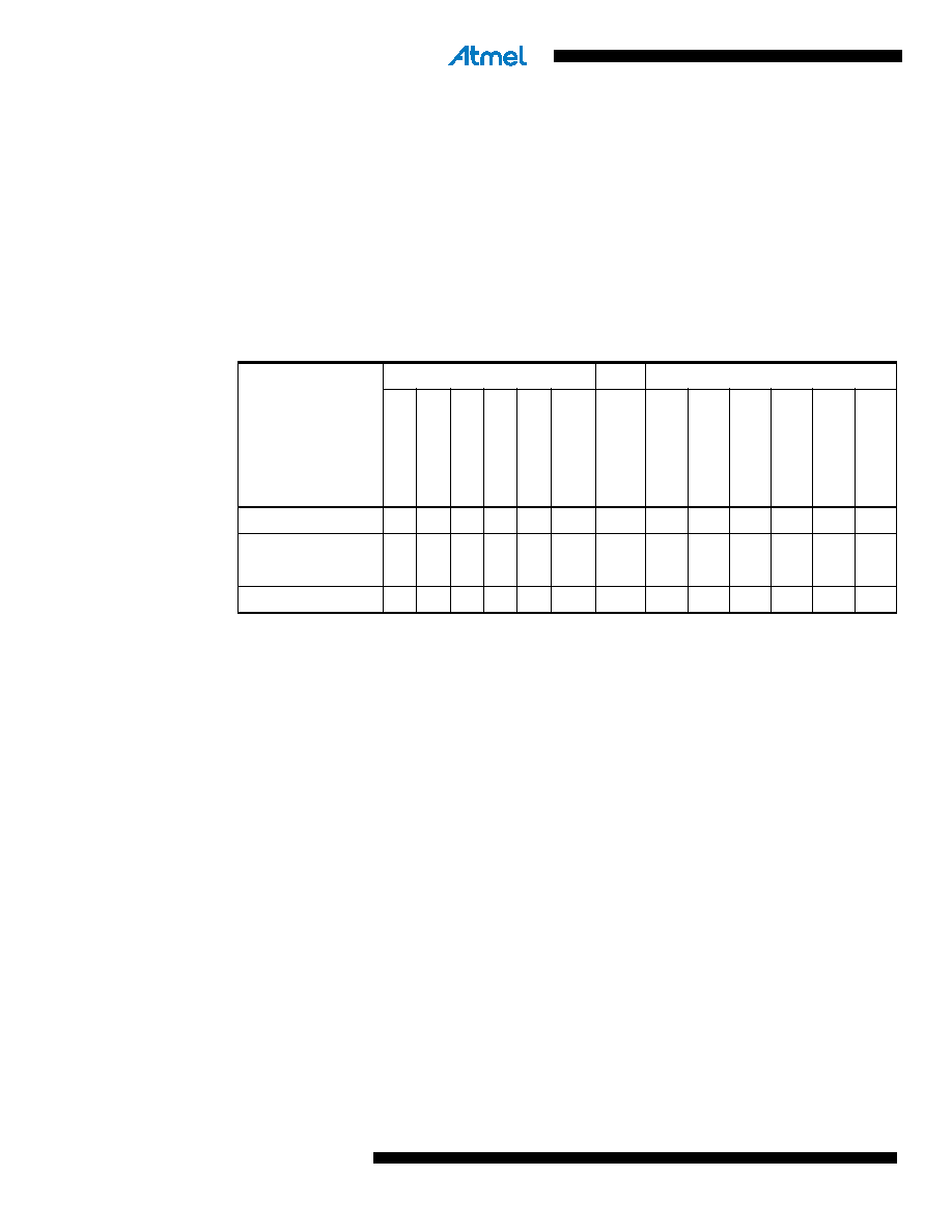
Table 7-1.
Active Clock Domains and Wake-up Sources in Different Sleep Modes
Sleep Mode
Active Clock Domains
Osc.
Wake-up Sources
clk
CP
U
clk
FLASH
clk
IO
clk
AD
C
clk
PC
K
clk
PLL
Main
Clo
ck
Source
Enab
led
IN
T0,
INT
1
and
Pin
Cha
nge
SPM
/EEPROM
Read
y
Interrupt
ADC
In
te
rru
p
t
USI
In
te
rru
p
t
Other
I/
O
W
a
tch
dog
In
te
rru
p
t
Idle
XXX
X(2)
X
XXXX
ADC Noise Reduct.
X
X(2)
XX(1)
XX
X
Power-down
X(1)
XX
Standby
X(1)
XX
相关PDF资料 |
PDF描述 |
|---|---|
| R5F2L38ACNFA | 8-BIT, FLASH, 20 MHz, MICROCONTROLLER, PQFP80 |
| R5F2L38CCNFP | 8-BIT, FLASH, 20 MHz, MICROCONTROLLER, PQFP80 |
| R5F2L387CDFP | 8-BIT, FLASH, 20 MHz, MICROCONTROLLER, PQFP80 |
| R5F2L387CNFP | 8-BIT, FLASH, 20 MHz, MICROCONTROLLER, PQFP80 |
| R5F2L368CDFP | 8-BIT, FLASH, 20 MHz, MICROCONTROLLER, PQFP64 |
相关代理商/技术参数 |
参数描述 |
|---|---|
| R5F2L3ACCNFP#30 | 制造商:Renesas Electronics Corporation 功能描述:IC MCU 16BIT 128KB FLASH 100LQFP |
| R5F2L3ACCNFP#U1 | 制造商:Renesas Electronics Corporation 功能描述: |
| R5F2L3ACCNFP#V0 | 功能描述:MCU 1KB FLASH 128K ROM 100-LQFP RoHS:是 类别:集成电路 (IC) >> 嵌入式 - 微控制器, 系列:R8C/Lx/3AC 标准包装:250 系列:80C 核心处理器:8051 芯体尺寸:8-位 速度:16MHz 连通性:EBI/EMI,I²C,UART/USART 外围设备:POR,PWM,WDT 输入/输出数:40 程序存储器容量:- 程序存储器类型:ROMless EEPROM 大小:- RAM 容量:256 x 8 电压 - 电源 (Vcc/Vdd):4.5 V ~ 5.5 V 数据转换器:A/D 8x10b 振荡器型:内部 工作温度:-40°C ~ 85°C 封装/外壳:68-LCC(J 形引线) 包装:带卷 (TR) |
| R5F2L3ACMDFA#U0 | 制造商:Renesas Electronics Corporation 功能描述:R8C/L3AM 128+4/10 100QFP 14X20 制造商:Renesas Electronics Corporation 功能描述:R8C/L3AM 128+4/10 100QFP 14X20 -40 TO +85 - Trays 制造商:Renesas Electronics Corporation 功能描述:IC MCU 16BIT 128KB FLASH 100LQFP |
| R5F2L3ACMNFA#U0 | 制造商:Renesas Electronics Corporation 功能描述:R8C/L3AM 128+4/10 100QFP 14X20 制造商:Renesas Electronics Corporation 功能描述:R8C/L3AM 128+4/10 100QFP 14X20 -20 TO +85 - Trays 制造商:Renesas Electronics Corporation 功能描述:IC MCU 16BIT 128KB FLASH 100LQFP 制造商:Renesas Electronics Corporation 功能描述:MCU,R8C,16bit,20MHz,128KB Flash,QFP100 |
发布紧急采购,3分钟左右您将得到回复。