- 您现在的位置:买卖IC网 > PDF目录11066 > R5F5630ADDFP#V0 (Renesas Electronics America)MCU RX630 768KB FLASH 100-LQFP PDF资料下载
参数资料
| 型号: | R5F5630ADDFP#V0 |
| 厂商: | Renesas Electronics America |
| 文件页数: | 28/165页 |
| 文件大小: | 0K |
| 描述: | MCU RX630 768KB FLASH 100-LQFP |
| 产品培训模块: | RX Compare Match Timer RX DMAC |
| 标准包装: | 1 |
| 系列: | RX600 |
| 核心处理器: | RX |
| 芯体尺寸: | 32-位 |
| 速度: | 100MHz |
| 连通性: | CAN,EBI/EMI,I²C,LIN,SCI,SPI,USB |
| 外围设备: | DMA,LVD,POR,PWM,WDT |
| 输入/输出数: | 78 |
| 程序存储器容量: | 768KB(768K x 8) |
| 程序存储器类型: | 闪存 |
| RAM 容量: | 96K x 8 |
| 电压 - 电源 (Vcc/Vdd): | 2.7 V ~ 3.6 V |
| 数据转换器: | A/D 8x10b,14x12b,D/A 1x10b |
| 振荡器型: | 内部 |
| 工作温度: | -40°C ~ 85°C |
| 封装/外壳: | 100-LQFP |
| 包装: | 托盘 |
第1页第2页第3页第4页第5页第6页第7页第8页第9页第10页第11页第12页第13页第14页第15页第16页第17页第18页第19页第20页第21页第22页第23页第24页第25页第26页第27页当前第28页第29页第30页第31页第32页第33页第34页第35页第36页第37页第38页第39页第40页第41页第42页第43页第44页第45页第46页第47页第48页第49页第50页第51页第52页第53页第54页第55页第56页第57页第58页第59页第60页第61页第62页第63页第64页第65页第66页第67页第68页第69页第70页第71页第72页第73页第74页第75页第76页第77页第78页第79页第80页第81页第82页第83页第84页第85页第86页第87页第88页第89页第90页第91页第92页第93页第94页第95页第96页第97页第98页第99页第100页第101页第102页第103页第104页第105页第106页第107页第108页第109页第110页第111页第112页第113页第114页第115页第116页第117页第118页第119页第120页第121页第122页第123页第124页第125页第126页第127页第128页第129页第130页第131页第132页第133页第134页第135页第136页第137页第138页第139页第140页第141页第142页第143页第144页第145页第146页第147页第148页第149页第150页第151页第152页第153页第154页第155页第156页第157页第158页第159页第160页第161页第162页第163页第164页第165页
R01DS0060EJ0100 Rev.1.00
Page 123 of 168
Sep 13, 2011
RX630 Group
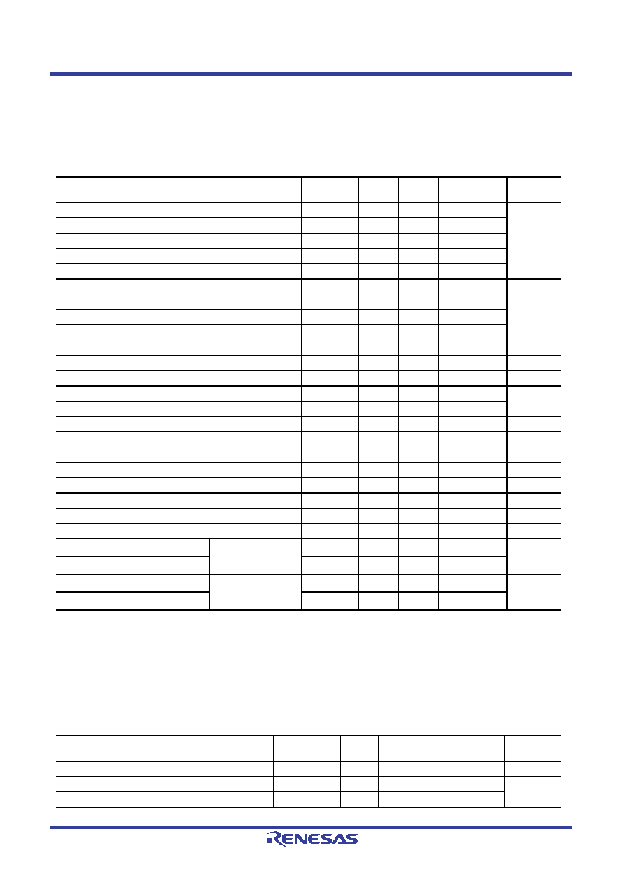
5. Electrical Characteristics
5.4
Clock Timing
Note 1. This is the time until the clock is used after setting P36 and P37 as inputs, and then clearing the main clock-oscillator stop bit
(MOSCCR.MOSTP) to 0 (selecting operation).
Note 2. This is the time until the frequency of oscillation by the HOCO (fHOCO) reaches the range for guaranteed operation. after
release from the reset state.
Table 5.9
Clock Timing (Except for Sub-Clock Related)
Conditions: VCC = AVCC0 = VCC_USB = VBATT = 2.7 to 3.6 V, VREFH/VREFH0 = 2.7 V to AVCC0,
VSS = AVSS0 = VREFL/VREFL0 = VSS_USB = 0 V, Ta = Topr
Item
Symbol
Min.
Typ.
Max.
Unit
Test
Conditions
BCLK pin output cycle time
tBcyc
40
—
ns
BCLK pin output high pulse width
tCH
5—
—
ns
BCLK pin output low pulse width
tCL
5—
—
ns
BCLK pin output rising time
tCr
——
5
ns
BCLK pin output falling time
tCf
——
5
ns
EXTAL external clock input cycle time
tEXcyc
50
—
ns
EXTAL external clock input high pulse width
tEXH
20
—
ns
EXTAL external clock input low pulse width
tEXL
20
—
ns
EXTAL external clock rising time
tEXr
——
5
ns
EXTAL external clock falling time
tEXf
——
5
ns
EXTAL external clock input wait time*1
tEXWT
1—
—
ms
Main clock oscillator oscillation frequency
fMAIN
4
—
16
MHz
Main clock oscillation stabilization time (crystal)
tMAINOSC
10
—
ms
Main clock oscillation stabilization wait time (crystal)
tMAINOSCWT
20
—
ms
LOCO clock cycle time
tcyc
9.4
8
6.96
s
Low-speed on-chip oscillator oscillation frequency
fLOCO
106.25
125
143.75
kHz
LOCO clock oscillation stabilization wait time
tLOCOWT
—
20
s
High-speed on-chip oscillator oscillation frequency
fHOCO
45
50
55
MHz
HOCO clock oscillation stabilization wait time 1*2
tHOCOWT1
—
1.8
ms
HOCO clock oscillation stabilization wait time 2
tHOCOWT2
—
2.0
ms
HOCO clock power supply settling time
tHOCOP
—
1
ms
PLL circuit oscillation frequency
fPLL
104
—
200
MHz
PLL clock oscillation stabilization time
PLL operation started
after main clock
oscillation has settled
tPLL1
—
500
s
PLL clock oscillation stabilization wait
tPLLWT1
1.5
—
ms
PLL clock oscillation stabilization time
PLL operation started
before main clock
oscillation has settled
tPLL2
10
—
ms
PLL clock oscillation stabilization wait
tPLLWT2
11
—
ms
Table 5.10
Clock Timing (Sub-Clock Related)
Conditions: VCC = AVCC0 = VCC_USB = 2.7 to 3.6 V, VREFH/VREFH0 = 2.7 V to AVCC0, VBATT = 2.3 to 3.6 V,
VSS = AVSS0 = VREFL/VREFL0 = VSS_USB = 0 V, Ta = Topr
Item
Symbol
Min.
Typ.
Max.
Unit
Test
Conditions
Sub-clock oscillator oscillation frequency
fSUB
—
32.768
—
kHz
Sub-clock oscillation stabilization time
tSUBOSC
2
—
s
Sub-clock oscillation stabilization wait time
tSUBOSCWT
4—
—
s
相关PDF资料 |
PDF描述 |
|---|---|
| DF36034GFPWV | IC H8/36034 MCU FLASH 64LQFP |
| VI-244-IY-F1 | CONVERTER MOD DC/DC 48V 50W |
| VI-243-IY-F4 | CONVERTER MOD DC/DC 24V 50W |
| VI-243-IY-F3 | CONVERTER MOD DC/DC 24V 50W |
| VI-243-IY-F1 | CONVERTER MOD DC/DC 24V 50W |
相关代理商/技术参数 |
参数描述 |
|---|---|
| R5F5630ADDLC | 制造商:RENESAS 制造商全称:Renesas Technology Corp 功能描述:Renesas MCUs |
| R5F5630ADDLC#U0 | 制造商:Renesas Electronics Corporation 功能描述:RX630 768KB/96KB LGA177 CAN 100MHZ - Trays |
| R5F5630ADDLK | 制造商:RENESAS 制造商全称:Renesas Technology Corp 功能描述:Renesas MCUs |
| R5F5630ADDLK#U0 | 制造商:Renesas Electronics Corporation 功能描述:RX630 768KB/96KB LGA145 CAN 100MHZ - Trays |
| R5F5630BCDBG | 制造商:RENESAS 制造商全称:Renesas Technology Corp 功能描述:Renesas MCUs |
发布紧急采购,3分钟左右您将得到回复。