- 您现在的位置:买卖IC网 > PDF目录230922 > RD-19240FG-200T (DATA DEVICE CORP) SYNCHRO OR RESOLVER TO DIGITAL CONVERTER, PQFP52 PDF资料下载
参数资料
| 型号: | RD-19240FG-200T |
| 厂商: | DATA DEVICE CORP |
| 元件分类: | 位置变换器 |
| 英文描述: | SYNCHRO OR RESOLVER TO DIGITAL CONVERTER, PQFP52 |
| 封装: | 10 X 10 MM, ROHS COMPLIANT, PLASTIC, MQFP-52 |
| 文件页数: | 15/19页 |
| 文件大小: | 432K |
| 代理商: | RD-19240FG-200T |
5
Data Device Corporation
www.ddc-web.com
RD-19240
F-0209-0
ERROR PROCESSOR
RESOLVER
INPUT
(
θ)
VELOCITY
OUT
DIGITAL
POSITION
OUT (
φ)
VCO
CT
S
A
+ 1
1
B
S
+ 1
10B
H = 1
+
-
e
A2
S
-12
db/oct
BA
2A
-6 db/oct
10B
ω (rad/sec)
2A
2 2 A
ω (rad/sec)
f
= BW (Hz) =
BW
2 A
π
CLOSED LOOP
(B = A/2)
GAIN = 0.4
GAIN = 4
(CRITICALLY DAMPED)
OPEN LOOP
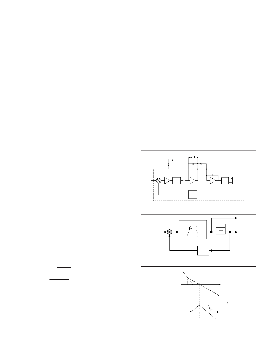
FIGURE 3. TRANSFER FUNCTION BLOCK DIAGRAM #2
FIGURE 4. BODE PLOTS
The error processing is performed using the industry standard
technique for type II tracking R/D converters. The DC error is
integrated yielding a velocity voltage which in turn drives a volt-
age-controlled oscillator (VCO). This VCO is an incremental inte-
grator (constant voltage input to position rate output) which,
together with the velocity integrator, forms a type II servo feed-
back loop. A lead in the frequency response is introduced to sta-
bilize the loop, and a lag at higher frequency is introduced to
reduce the gain and ripple at the carrier frequency and above.
The settings of the various error processor gains and break fre-
quencies are done with external resistors and capacitors so that
the converter loop dynamics can be easily controlled by the user.
Dynamic accuracy may be degraded in applications with a high
system bandwidth. This error is more likely to be seen when the A-
quad-B signals are used in systems that have high bandwidths
and as such may affect system performance accordingly such as
encoder applications.This dynamic accuracy error is usually not an
issue when using the RD-19240’s analog velocity output or posi-
tion output data in a control-loop because they are inherently fil-
tered due to comparatively low bandwidths in most applications.
TRANSFER FUNCTION AND BODE PLOT
The dynamic performance of the converter can be determined
from its Transfer Function Block Diagrams and its Bode Plots
(open and closed loop). These are shown in FIGURES 2, 3, and 4.
The open loop transfer function is as follows:
where:
A is the gain coefficient
A2 = A
1A2
B is the frequency of lead compensation
The components of gain coefficient are error gradient, integrator
gain, and VCO gain. These can be broken down as follows:
where:
C
s = 10 pF
F
s = 70 kHz when Rs = 30 kΩ
F
s = 100 kHz when Rs = 20 kΩ
F
s = 125 kHz when Rs = 15 kΩ
C
vco = 50 pF
- Error Gradient = 0.011 volts per LSB (CT+Error
Amp+Demod with 2 Vrms input)
- Integrator gain =
volts per second per volt
- VCO Gain =
LSBs per second per volt
1
1.25 R
vCvco
C
SFS
1.1C
BW
Open Loop Transfer Function =
A
(S
B
+ 1
)
2
S
( S
10B
+ 1
)
2
GAIN
11 mV/LSB
16 BIT
UP/DOWN
COUNTER
R1
VCO
RV
RB CBW
C
/10
BW
VEL
-VCO
H = 1
-VSUM
VEL
C F
S S
CT
+
-
RESOLVER
INPUT
(
θ)
RS
50 pf
CVCO
DIGITAL
OUTPUT
(
φ)
DEMOD
±1.25 V
THRESHOLD
1
FIGURE 2. TRANSFER FUNCTION BLOCK DIAGRAM #1
(Fs = internal sample frequency)
R
V, RB, and CBW are selected by the user to set velocity scaling
and bandwidth.
GENERAL SETUP CONDITIONS
DDC has external component selection software that considers all
the criteria below and, in a simple fashion, asks the key parame-
ters (carrier frequency, resolution, bandwidth, and tracking rate) to
derive the external component values. For detailed setup informa-
tion refer to the RD/RDC Series Converters Applications Manual
(document #MN-19220XX-001) available at www.ddc-web.com.
The following recommendations should be considered when
installing the RD-19240 Resolver-to-Digital (R/D) converter:
1) When setting the bandwidth (BW) and Tracking Rate (TR)
(selecting five external components), the system require-
ments need to be considered. For the greatest noise immuni-
ty, select the minimum BW and TR the system will allow.
相关PDF资料 |
PDF描述 |
|---|---|
| RD-14597F1-824S | SYNCHRO OR RESOLVER TO DIGITAL CONVERTER, CDFP36 |
| RDC-19220S-403Z | SYNCHRO OR RESOLVER TO DIGITAL CONVERTER, CDIP40 |
| RDC-19220S-422K | SYNCHRO OR RESOLVER TO DIGITAL CONVERTER, CDIP40 |
| RDC-19220S-422L | SYNCHRO OR RESOLVER TO DIGITAL CONVERTER, CDIP40 |
| RD-14597F1-234L | SYNCHRO OR RESOLVER TO DIGITAL CONVERTER, CDFP36 |
相关代理商/技术参数 |
参数描述 |
|---|---|
| RD1-9320 | 制造商:STMicroelectronics 功能描述:MPU DEMO-BOARD |
| RD1950MPXM2010GS | 制造商:Freescale Semiconductor 功能描述:WATER LEVEL REFERENCE DESIGN - Bulk |
| RD1986MMA2260D | 功能描述:加速传感器开发工具 TRIAX REF DSGN 3-AXIS FOR MMA2260D RoHS:否 制造商:Murata 工具用于评估:SCA3100-D04 加速:2 g 传感轴:Triple Axis 接口类型:SPI 工作电压:3.3 V |
| RD1986MMA6260Q | 功能描述:加速传感器开发工具 TRIAX REF DSGN 3-AXIS FOR NMA6260Q RoHS:否 制造商:Murata 工具用于评估:SCA3100-D04 加速:2 g 传感轴:Triple Axis 接口类型:SPI 工作电压:3.3 V |
| RD1A-12S | 制造商:World Products 功能描述: |
发布紧急采购,3分钟左右您将得到回复。