- 您现在的位置:买卖IC网 > PDF目录230922 > RD-19240FG-200T (DATA DEVICE CORP) SYNCHRO OR RESOLVER TO DIGITAL CONVERTER, PQFP52 PDF资料下载
参数资料
| 型号: | RD-19240FG-200T |
| 厂商: | DATA DEVICE CORP |
| 元件分类: | 位置变换器 |
| 英文描述: | SYNCHRO OR RESOLVER TO DIGITAL CONVERTER, PQFP52 |
| 封装: | 10 X 10 MM, ROHS COMPLIANT, PLASTIC, MQFP-52 |
| 文件页数: | 3/19页 |
| 文件大小: | 432K |
| 代理商: | RD-19240FG-200T |
11
Data Device Corporation
www.ddc-web.com
RD-19240
F-0209-0
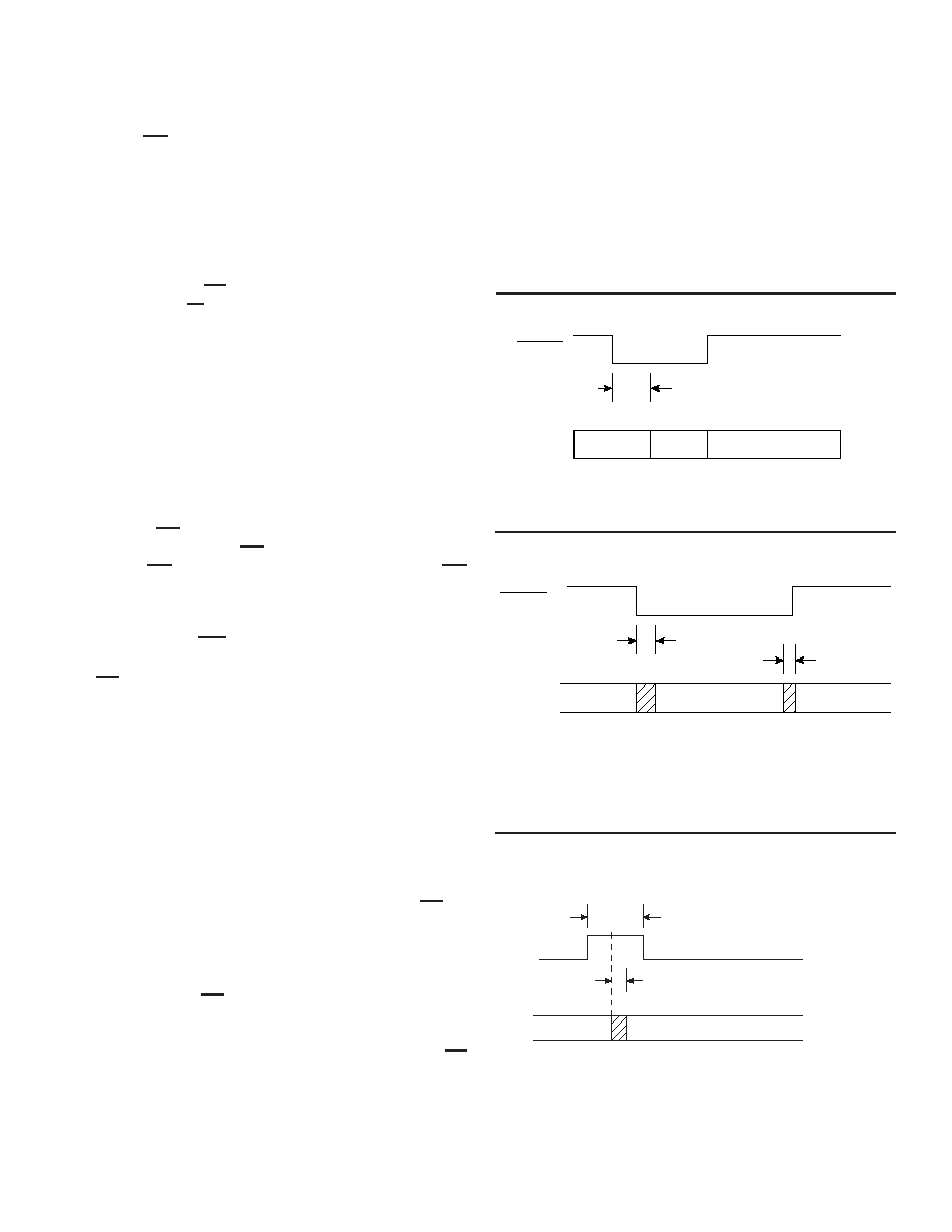
INHIBIT, ENABLE, AND CB TIMING
The Inhibit (INH) signal is used to freeze the digital output angle
in the transparent output data latch while data is being trans-
ferred. Application of an inhibit signal does not interfere with the
continuous tracking of the converter. As shown in FIGURE 12,
angular output data is valid 150 ns maximum after the applica-
tion of the negative inhibit pulse.
Output angle data is enabled onto the tri-state data bus in two
bytes. Enable MSBs (EM) is used for the most significant 8 bits
and Enable LSBs (EL) is used for the least significant 6 bits. As
shown in FIGURE 13, output data is valid 150 ns maximum after
the application of a negative enable pulse. The tri-state data bus
returns to the high impedance state 100 ns maximum after the
rising edge of the enable signal.
The Converter Busy (CB) signal indicates that the tracking con-
verter output angle is changing 1 LSB. As shown in FIGURE 14,
output data is valid 50 ns maximum after the middle of the CB
pulse. The CB pulse width is 1/(40 x Fs), which is nominally 375
ns.
Note that the INH signal may be applied regardless of the logic
state of the CB signal. If an INH signal is applied and the CB line
is busy, the INH will wait for CB timing before setting the INH
latch as per FIGURE 14.
BUILT-IN-TEST (BIT)
The BIT output is active low, and is triggered if any of the follow-
ing conditions exist:
1) Loss of Signal (LOS) - Sin and Cos inputs are both less than
500mV. The LOS has a filter on it to filter out the reference.
Time constants of 50 ms or more are possible.
2) Loss of Reference (LOR) - Reference Input less than 500 mV.
3) Excessive Error - This error is detected by monitoring the
demodulator output, which is proportional to the difference
between the analog input and digital output. When it exceeds
approximately 100 LSBs (in the selected resolution), BIT will
be asserted. This condition can occur any time the analog
input changes at a rate in excess of the maximum tracking
rate. During power up, the converter may see a large differ-
ence between the sin/cos inputs and the digital output angle
held in its counter. BIT will be asserted until the converter set-
tles within ~ 100 LSB’s of the final result.
A 500 s dynamic delay occurs before the excessive error BIT
becomes active. This dynamic delay is responsive to the
active filter loop.
During normal operation, for step inputs, or on power up, a
large error can exist.
4) 180° phase error input signal to reference input (false null)
causes a BIT plus kickstarts the converter counter to correct
the error.
;;
;;;
DATA
VALID
150 ns max
INHIBIT
100 ns MAX
ENABLE
150 ns MAX
DATA
VALID
HIGH Z
For 16 bit bus, EM and EL may be tied to ground for transparent mode,
providing only one 16 bit R/D channel is on the data bus.
1/(40 x Fs)
(375 nsec nominal)
CB
50 ns
DATA
VALID
DATA
VALID
*
* Next CB pulse
cannot occur for
a minimum of
150 nsec.
FIGURE 12. INHIBIT TIMING
FIGURE 13. ENABLE TIMING
FIGURE 14. CONVERTER BUSY TIMING
相关PDF资料 |
PDF描述 |
|---|---|
| RD-14597F1-824S | SYNCHRO OR RESOLVER TO DIGITAL CONVERTER, CDFP36 |
| RDC-19220S-403Z | SYNCHRO OR RESOLVER TO DIGITAL CONVERTER, CDIP40 |
| RDC-19220S-422K | SYNCHRO OR RESOLVER TO DIGITAL CONVERTER, CDIP40 |
| RDC-19220S-422L | SYNCHRO OR RESOLVER TO DIGITAL CONVERTER, CDIP40 |
| RD-14597F1-234L | SYNCHRO OR RESOLVER TO DIGITAL CONVERTER, CDFP36 |
相关代理商/技术参数 |
参数描述 |
|---|---|
| RD1-9320 | 制造商:STMicroelectronics 功能描述:MPU DEMO-BOARD |
| RD1950MPXM2010GS | 制造商:Freescale Semiconductor 功能描述:WATER LEVEL REFERENCE DESIGN - Bulk |
| RD1986MMA2260D | 功能描述:加速传感器开发工具 TRIAX REF DSGN 3-AXIS FOR MMA2260D RoHS:否 制造商:Murata 工具用于评估:SCA3100-D04 加速:2 g 传感轴:Triple Axis 接口类型:SPI 工作电压:3.3 V |
| RD1986MMA6260Q | 功能描述:加速传感器开发工具 TRIAX REF DSGN 3-AXIS FOR NMA6260Q RoHS:否 制造商:Murata 工具用于评估:SCA3100-D04 加速:2 g 传感轴:Triple Axis 接口类型:SPI 工作电压:3.3 V |
| RD1A-12S | 制造商:World Products 功能描述: |
发布紧急采购,3分钟左右您将得到回复。