- 您现在的位置:买卖IC网 > Datasheet目录354 > RDK-242 (Power Integrations)KIT REF DESIGN VG TOPSWITCH-JX Datasheet资料下载
参数资料
| 型号: | RDK-242 |
| 厂商: | Power Integrations |
| 文件页数: | 7/40页 |
| 文件大小: | 0K |
| 描述: | KIT REF DESIGN VG TOPSWITCH-JX |
| 标准包装: | 1 |
| 系列: | TOPSwitch®-JX |
| 主要目的: | AC/DC,主面和辅面 |
| 输出及类型: | 1,隔离 |
| 功率 - 输出: | 30W |
| 输出电压: | 12V |
| 电流 - 输出: | 2.5A |
| 输入电压: | 85 ~ 264VAC |
| 稳压器拓扑结构: | 回扫 |
| 频率 - 开关: | 132kHz |
| 板类型: | 完全填充 |
| 已供物品: | 板 |
| 已用 IC / 零件: | TOP266VG |
| 其它名称: | 596-1312 |
第1页第2页第3页第4页第5页第6页当前第7页第8页第9页第10页第11页第12页第13页第14页第15页第16页第17页第18页第19页第20页第21页第22页第23页第24页第25页第26页第27页第28页第29页第30页第31页第32页第33页第34页第35页第36页第37页第38页第39页第40页
�� �
�
�TOP264-271�
�V� UV�
�V� LINE�
�0V�
�S15�
�S14�
�S13� S12�
�S0�
�S15� S14�
�S13�
�S12�
�S0�
�S15�
�S14�
�S13�
�S12�
�S0�
�S15�
�S15�
�5.8� V�
�V� C�
�0V�
�V� DRAIN�
�0V�
�V� OUT�
�0V�
�4.8� V�
�1�
�2�
�3�
�2�
�4�
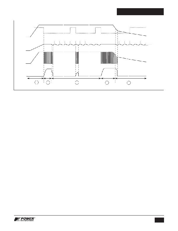
�Note:� S0� through� S15� are� the� output� states� of� the� auto-restart� counter�
�PI-4531-121206�
�Figure� 8.�
�Typical� Waveforms� for� (1)� Power� Up� (2)� Normal� Operation� (3)� Auto-Restart� (4)� Power� Down.�
�UV� prevents� auto-restart� attempts� after� the� output� goes� out� of�
�regulation.� This� eliminates� power� down� glitches� caused� by� slow�
�discharge� of� the� large� input� storage� capacitor� present� in�
�applications� such� as� standby� supplies.� A� single� resistor�
�connected� from� the� VOLTAGE-MONITOR� pin� to� the� rectified� DC�
�high-voltage� bus� sets� UV� threshold� during� power� up.� Once� the�
�power� supply� is� successfully� turned� on,� the� UV� threshold� is�
�lowered� to� 44%� of� the� initial� UV� threshold� to� allow� extended�
�input� voltage� operating� range� (UV� low� threshold).� If� the� UV� low�
�threshold� is� reached� during� operation� without� the� power� supply�
�losing� regulation,� the� device� will� turn� off� and� stay� off� until� UV�
�(high� threshold)� has� been� reached� again.� If� the� power� supply�
�loses� regulation� before� reaching� the� UV� low� threshold,� the�
�device� will� enter� auto-restart.� At� the� end� of� each� auto-restart�
�cycle� (S15),� the� UV� comparator� is� enabled.� If� the� UV� high�
�threshold� is� not� exceeded,� the� MOSFET� will� be� disabled� during�
�the� next� cycle� (see� Figure� 8).� The� UV� feature� can� be� disabled�
�independent� of� the� OV� feature.�
�Line� Overvoltage� Shutdown� (OV)�
�The� same� resistor� used� for� UV� also� sets� an� overvoltage�
�threshold,� which,� once� exceeded,� will� force� TOP264-271� to�
�stop� switching� instantaneously� (after� completion� of� the� current�
�switching� cycle).� If� this� condition� lasts� for� at� least� 100� m� s,� the�
�TOP264-271� output� will� be� forced� into� off� state.� When� the� line�
�voltage� is� back� to� normal� with� a� small� amount� of� hysteresis�
�provided� on� the� OV� threshold� to� prevent� noise� triggering,� the�
�state� machine� sets� to� S13� and� forces� TOP264-271� to� go�
�through� the� entire� auto-restart� sequence� before� attempting� to�
�switch� again.� The� ratio� of� OV� and� UV� thresholds� is� preset� at�
�4.5,� as� can� be� seen� in� Figure� 9.� When� the� MOSFET� is� off,� the�
�rectified� DC� high-voltage� surge� capability� is� increased� to� the�
�voltage� rating� of� the� MOSFET� (725� V),� due� to� the� absence� of� the�
�reflected� voltage� and� leakage� spikes� on� the� drain.� The� OV�
�feature� can� be� disabled� independent� of� the� UV� feature.�
�www.powerint.com�
�In� order� to� reduce� the� no-load� input� power� of� TOP264-271�
�designs,� the� V� pin� operates� at� very� low� currents.� This� requires�
�careful� layout� considerations� when� designing� the� PCB� to� avoid�
�noise� coupling.� Traces� and� components� connected� to� the� V� pin�
�should� not� be� adjacent� to� any� traces� carrying� switching� currents.�
�These� include� the� drain,� clamp� network,� bias� winding� return� or�
�power� traces� from� other� converters.� If� the� line� sensing� features�
�are� used,� then� the� sense� resistors� must� be� placed� within� 10� mm�
�of� the� V� pin� to� minimize� the� V� pin� node� area.� The� DC� bus�
�should� then� be� routed� to� the� line� sense� resistors.� Note� that�
�external� capacitance� must� not� be� connected� to� the� V� pin� as� this�
�may� cause� misoperation� of� the� V� pin� related� functions.�
�Hysteretic� or� Latching� Output� Overvoltage� Protection� (OVP)�
�The� detection� of� the� hysteretic� or� latching� output� overvoltage�
�protection� (OVP)� is� through� the� trigger� of� the� line� overvoltage�
�threshold.� The� V� pin� voltage� will� drop� by� 0.5� V,� and� the�
�controller� measures� the� external� attached� impedance� immediately�
�after� this� voltage� drops.� If� I� V� exceeds� I� OV(LS)� (336� m� A� typical)�
�longer� than� 100� m� s,� TOP264-271� will� latch� into� a� permanent� off�
�state� for� the� latching� OVP.� It� only� can� be� reset� if� I� X� exceeds� I� X(TH)�
�=� -27� m� A� (typ)� or� V� C� goes� below� the� power-up-reset� threshold�
�(V� C(RESET)� )� and� then� back� to� normal.� If� I� V� does� not� exceed� I� OV(LS)� or�
�exceeds� no� longer� than� 100� m� s,� TOP264-271� will� initiate� the� line�
�overvoltage� and� the� hysteretic� OVP.� Their� behavior� will� be�
�identical� to� the� line� overvoltage� shutdown� (OV)� that� has� been�
�described� in� detail� in� the� previous� section.� During� a� fault�
�condition� resulting� from� loss� of� feedback,� output� voltage� will�
�rapidly� rise� above� the� nominal� voltage.� The� increase� in� output�
�voltage� will� also� result� in� an� increase� in� the� voltage� at� the� output�
�of� the� bias� winding.� A� voltage� at� the� output� of� the� bias� winding�
�that� exceeds� of� the� sum� of� the� voltage� rating� of� the� Zener� diode�
�connected� from� the� bias� winding� output� to� the� V� pin� and� V� pin�
�voltage,� will� cause� a� current� in� excess� of� I� V� to� be� injected� into�
�the� V� pin,� which� will� trigger� the� OVP� feature.�
�7�
�Rev.� E� 08/12�
�相关PDF资料 |
PDF描述 |
|---|---|
| RJCSE538001 | CONN MOD JACK 8P8C SMT R/A |
| RJE031882420 | CONN MOD JACK 8P/8C S-FLANGES |
| RJE051660310 | CONN MOD JACK 6P/6C UNSHIELDED |
| RJE051880110 | CONN MOD JACK 8/8 R/A UNSHIELDED |
| RJE051881310 | CONN MOD JACK 8P/8C SHIELDED |
相关代理商/技术参数 |
参数描述 |
|---|---|
| RDK-248 | 功能描述:LED 照明开发工具 UNIVERSAL PFC 180W HiperPFS KIT RoHS:否 制造商:Fairchild Semiconductor 产品:Evaluation Kits 用于:FL7732 核心: 电源电压:120V 系列: 封装: |
| RDK-249 | 功能描述:线性和开关式电源 HiperTFS Ref Des Kit 14.W Stby, 300W PS RoHS:否 制造商:TDK-Lambda 产品:Switching Supplies 开放式框架/封闭式:Enclosed 输出功率额定值:800 W 输入电压:85 VAC to 265 VAC 输出端数量:1 输出电压(通道 1):20 V 输出电流(通道 1):40 A 商用/医用: 输出电压(通道 2): 输出电流(通道 2): 安装风格:Rack 长度: 宽度: 高度: |
| RDK-251 | 功能描述:LED 照明开发工具 LinkSwitch-PL Ref Des Kit, 5W Dim RoHS:否 制造商:Fairchild Semiconductor 产品:Evaluation Kits 用于:FL7732 核心: 电源电压:120V 系列: 封装: |
| RDK-252 | 功能描述:电源管理IC开发工具 CAPZero Ref Des Kit CAPZero RoHS:否 制造商:Maxim Integrated 产品:Evaluation Kits 类型:Battery Management 工具用于评估:MAX17710GB 输入电压: 输出电压:1.8 V |
| RDK-257 | 功能描述:LED 照明开发工具 RefDesign 12W90-265V LinkSwitch-PH RoHS:否 制造商:Fairchild Semiconductor 产品:Evaluation Kits 用于:FL7732 核心: 电源电压:120V 系列: 封装: |
发布紧急采购,3分钟左右您将得到回复。