- 您现在的位置:买卖IC网 > PDF目录69323 > RN80532KC0411M (INTEL CORP) 2000 MHz, MICROPROCESSOR, CPGA603 PDF资料下载
参数资料
| 型号: | RN80532KC0411M |
| 厂商: | INTEL CORP |
| 元件分类: | 微控制器/微处理器 |
| 英文描述: | 2000 MHz, MICROPROCESSOR, CPGA603 |
| 封装: | Interposer, Micro, PGA-603 |
| 文件页数: | 29/132页 |
| 文件大小: | 2316K |
| 代理商: | RN80532KC0411M |
第1页第2页第3页第4页第5页第6页第7页第8页第9页第10页第11页第12页第13页第14页第15页第16页第17页第18页第19页第20页第21页第22页第23页第24页第25页第26页第27页第28页当前第29页第30页第31页第32页第33页第34页第35页第36页第37页第38页第39页第40页第41页第42页第43页第44页第45页第46页第47页第48页第49页第50页第51页第52页第53页第54页第55页第56页第57页第58页第59页第60页第61页第62页第63页第64页第65页第66页第67页第68页第69页第70页第71页第72页第73页第74页第75页第76页第77页第78页第79页第80页第81页第82页第83页第84页第85页第86页第87页第88页第89页第90页第91页第92页第93页第94页第95页第96页第97页第98页第99页第100页第101页第102页第103页第104页第105页第106页第107页第108页第109页第110页第111页第112页第113页第114页第115页第116页第117页第118页第119页第120页第121页第122页第123页第124页第125页第126页第127页第128页第129页第130页第131页第132页
9-26
Intel Xeon Processor MP with up to 2MB L3 Cache
SM_EP_A[2:0]
I
The SM_EP_A (EEPROM Select Address) pins are decoded on the SMBus in
conjunction with the upper address bits in order to maintain unique addresses on
the SMBus in a system with multiple processors. To set an SM_EP_A line high, a
pull-up resistor should be used that is no larger than 1k
. The processor includes a
10k
pull-down resistor to V
SS for each of these signals. It is only available on the
Intel Xeon processor in INT-mPGA package.
For more information on the usage of these pins, see Section 6.4.8.
SM_TS_A[1:0]
I
The SM_TS_A (Thermal Sensor Select Address) pins are decoded on the SMBus
in conjunction with the upper address bits in order to maintain unique addresses on
the SMBus in a system with multiple processors.
The device’s addressing, as implemented, includes a Hi-Z state for both address
pins. The use of the Hi-Z state is achieved by leaving the input floating
(unconnected). It is only available on the Intel Xeon processor in INT-mPGA
package.
For more information on the usage of these pins, see Section 6.4.8.
SM_VCC
I
Provides power to the SMBus components which are only available on the Intel
Xeon processor in INT-mPGA package. Additionally provides power for the VID and
BSEL logic. Intel Xeon processor MP on the 0.13 micron processprocessor
baseboards MUST provide SM_Vcc. See Figure for further details.
SM_WP
I
WP (Write Protect) can be used to write protect the Scratch EEPROM. The Scratch
EEPROM is write-protected when this input is pulled high to SM_VCC.The
processor includes a 10k pull-down resistor to VSS for this signal. It is only available
on the Intel Xeon processor in INT-mPGA package.
SMI#
I
SMI# (System Management Interrupt) is asserted asynchronously by system logic.
On accepting a System Management Interrupt, processors save the current state
and enter System Management Mode (SMM). An SMI Acknowledge transaction is
issued, and the processor begins program execution from the SMM handler.
If SMI# is asserted during the deassertion of RESET# the processor will tri-state its
outputs. It is only available on the Intel Xeon processor in INT-mPGA package.
STPCLK#
I
STPCLK# (Stop Clock), when asserted, causes processors to enter a low power
Stop-Grant state. The processor issues a Stop-Grant Acknowledge transaction, and
stops providing internal clock signals to all processor core units except the system
bus and APIC units. The processor continues to snoop bus transactions and
service interrupts while in Stop-Grant state. When STPCLK# is deasserted, the
processor restarts its internal clock to all units and resumes execution. The
assertion of STPCLK# has no effect on the bus clock; STPCLK# is an
asynchronous input.
TCK
I
TCK (Test Clock) provides the clock input for the processor Test Bus (also known
as the Test Access Port).
TDI
I
TDI (Test Data In) transfers serial test data into the processor. TDI provides the
serial input needed for JTAG specification support.
TDO
O
TDO (Test Data Out) transfers serial test data out of the processor. TDO provides
the serial output needed for JTAG specification support.
TESTHI[6:0]
I
All TESTHI[6:0] pins should be individually connected to VCC via a pull-up resistor
which matches the trace impedance within a range of ± 10
. TESTHI[3:0] and
TESTHI[6:5] may all be tied together and pulled up to VCC with a single resistor if
desired. However, utilization of boundary scan test will not be functional if these
pins are connected together. TESTHI4 must always be pulled up independently
from the other TESTHI pins. For optimum noise margin, all pull-up resistor values
used for TESTHI[6:0] pins should have a resistance value within ± 20% of the
impedance of the baseboard transmission line traces. For example, if the trace
impedance is 50
, then a value between 40 and 60 should be used.
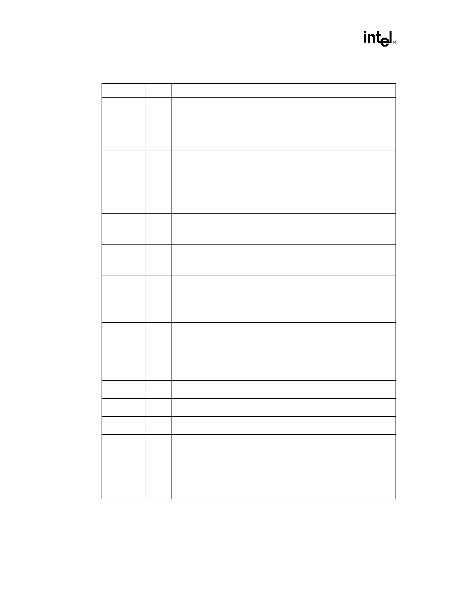
Table 52. Signal Definitions (Sheet 8 of 9)
Name
Type
Description
相关PDF资料 |
PDF描述 |
|---|---|
| RN80532KC0412M | 2000 MHz, MICROPROCESSOR, CPGA603 |
| RN80532KC041512 | 32-BIT, 2000 MHz, MICROPROCESSOR, CPGA603 |
| RP0352 | GRAPHICS PROCESSOR, PQFP80 |
| RP65C02G-06 | 8-BIT, 6 MHz, MICROPROCESSOR, PDIP40 |
| RPIXP2800BC | 32-BIT, 650 MHz, RISC PROCESSOR, PBGA1356 |
相关代理商/技术参数 |
参数描述 |
|---|---|
| RN80532KC041512 | 制造商:Intel 功能描述:TRAY XEON 2.0GHZ 400MZH FSB - Trays 制造商:Rochester Electronics LLC 功能描述:- Bulk |
| RN80532KC041512 SL5Z9 | 制造商:Intel 功能描述:MPU XEON 0.13UM 2GHZ 603-PIN UFCBGA - Trays |
| RN80532KC041512 SL6EM | 制造商:Intel 功能描述:MPU XEON 0.13UM 2GHZ 603-PIN UFCBGA - Trays |
| RN80532KC041512S L5Z9 | 制造商:Intel 功能描述:MPU Xeon? Processor 0.13um 2GHz 603-Pin uFCBGA |
| RN80532KC041512S L6W6 | 制造商:Intel 功能描述:MPU Xeon? Processor 0.13um 2GHz 603-Pin uFCBGA |
发布紧急采购,3分钟左右您将得到回复。