- 您现在的位置:买卖IC网 > PDF目录98069 > S1D13600F00A CRT OR FLAT PNL GRPH DSPL CTLR, PQFP64 PDF资料下载
参数资料
| 型号: | S1D13600F00A |
| 元件分类: | 显示控制器 |
| 英文描述: | CRT OR FLAT PNL GRPH DSPL CTLR, PQFP64 |
| 封装: | QFP6-64 |
| 文件页数: | 29/29页 |
| 文件大小: | 190K |
| 代理商: | S1D13600F00A |
第1页第2页第3页第4页第5页第6页第7页第8页第9页第10页第11页第12页第13页第14页第15页第16页第17页第18页第19页第20页第21页第22页第23页第24页第25页第26页第27页第28页当前第29页
S1D13600 Series
Rev. 2.3
EPSON
1–9
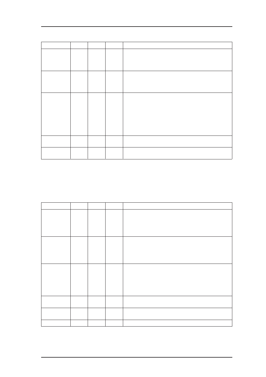
Table 3. SRAM Interface Pin Description
Pin Name
Type Pin No.
Drv
Description
T
The “VD [0:7]” signals are connected to SRAM’s 8
VD [0:7]
I/O
35…42 O2
bit data. The captured display data in S1D13600
PU
are stored in the SRAM through “VD [0:7]” by the
“VR/
W” signal.
The “VA [0:14]” signals are connected to SRAM’s
VA [0:14]
O
44…58 O2
address lines. “VA [0:14]” generate either CPU
Display Data Write Address or Display Refresh
Address depending upon operation modes.
S1D13600 manages up to 64 kb of SRAM as a
frame buffer memory. S1D13600 is configured to
primarily use two 256 kb SRAMs. “
VCS0” is
VCS [0:1]
O
59, 60
O2
active when 1st 32 kb is selected. “
VCS1” is
active when the rest 32 kb is selected. “
VCS
[0:1]” are connected to SRAM’s chip select inputs
(active LOW). Those signals are inactie (HIGH), if
the chip is in Sleep Mode.
VOE
O34
O2
The “
VOE” signal is connected to SRAM’s data
output enable input.
VR/
W
O43
O2
The “VR/
W” signal is connected to SRAM’s write
strobe input.
LCD Interface
The LCD interface signals are placed on the rest one side of the chip. The output type of all signals is
optimized to drive the Ultra Low Power LCD Module properly.
Pin Name
Type Pin No.
Drv
Description
The “XD [0:7]” signals are connected to the display
data inputs of the LCD Module. During Doze
XD [0:7]
O
24…31 O1
Mode, the signals are driven LOW. “XD [0:7] are
transferred to the LCD Module by the falling edge
of “XSCLU”.
The “XSCLU” signal is connected to the display
data shift clock of the LCD Module. During Doze
XSCLU
O
20
O1
Mode, the signal is driven LOW to force the RAM
integrated Segment Drivers to be in Power Save
Mode.
The “LP” signal is connected to te input, which
drives the data latching pulse of the segment
LP
O
21
O1
drivers and the scanning clock of the common
drivers, of the LCD Module. The “LP” period is
directly generated by the signal which is input
through “OSC1”.
YD
O
22
O1
The “YD” is connected to the frame start pulse
signal of the LCD Module.
FR
O
23
O1
The “FR” signal is connected to the signal which
alternates the LCD voltage in the LCD Module.
DOFF
O
18
O1
This signal outputs LOW if the chip is in Sleep Mode.
Table 4. LCD Interface Pin Description
相关PDF资料 |
PDF描述 |
|---|---|
| S1D13700F02A100 | 320 X 240 PIXELS CRT OR FLAT PNL GRPH DSPL CTLR, PQFP64 |
| S1D13706F00A | 320 X 240 PIXELS CRT OR FLAT PNL GRPH DSPL CTLR, PQFP100 |
| S1D13806F00A | CRT OR FLAT PNL GRPH DSPL CTLR, PQFP144 |
| S1D13A05B00B | 320 X 320 PIXELS CRT OR FLAT PNL GRPH DSPL CTLR, PBGA121 |
| S1D13A05F00A100 | 320 X 320 PIXELS CRT OR FLAT PNL GRPH DSPL CTLR, PBGA121 |
相关代理商/技术参数 |
参数描述 |
|---|---|
| S1D13700 | 制造商:EPSON 制造商全称:EPSON 功能描述:Embedded Memory Graphics LCD Controller |
| S1D13700F01A100 | 功能描述:显示驱动器和控制器 LCD CONTROLLER RoHS:否 制造商:Panasonic Electronic Components 工作电源电压:2.7 V to 5.5 V 最大工作温度: 安装风格:SMD/SMT 封装 / 箱体:QFN-44 封装:Reel |
| S1D13700F02A100 | 功能描述:显示驱动器和控制器 (QVGA) 320x240 B/W STN LCD C RoHS:否 制造商:Panasonic Electronic Components 工作电源电压:2.7 V to 5.5 V 最大工作温度: 安装风格:SMD/SMT 封装 / 箱体:QFN-44 封装:Reel |
| S1D13701F00A100 | 功能描述:LCD 驱动器 Organic EL Controller RoHS:否 制造商:Maxim Integrated 数位数量:4.5 片段数量:30 最大时钟频率:19 KHz 工作电源电压:3 V to 3.6 V 最大工作温度:+ 85 C 最小工作温度:- 20 C 封装 / 箱体:PDIP-40 封装:Tube |
| S1D13702F00A100 | 功能描述:LCD 驱动器 Organic EL Controller RoHS:否 制造商:Maxim Integrated 数位数量:4.5 片段数量:30 最大时钟频率:19 KHz 工作电源电压:3 V to 3.6 V 最大工作温度:+ 85 C 最小工作温度:- 20 C 封装 / 箱体:PDIP-40 封装:Tube |
发布紧急采购,3分钟左右您将得到回复。