- 您现在的位置:买卖IC网 > PDF目录98071 > S83C196MH (INTEL CORP) 16-BIT, MROM, 16 MHz, MICROCONTROLLER, PQFP80 PDF资料下载
参数资料
| 型号: | S83C196MH |
| 厂商: | INTEL CORP |
| 元件分类: | 微控制器/微处理器 |
| 英文描述: | 16-BIT, MROM, 16 MHz, MICROCONTROLLER, PQFP80 |
| 封装: | SHRINK, QFP-80 |
| 文件页数: | 13/41页 |
| 文件大小: | 1547K |
| 代理商: | S83C196MH |
第1页第2页第3页第4页第5页第6页第7页第8页第9页第10页第11页第12页当前第13页第14页第15页第16页第17页第18页第19页第20页第21页第22页第23页第24页第25页第26页第27页第28页第29页第30页第31页第32页第33页第34页第35页第36页第37页第38页第39页第40页第41页
8XC196MH INDUSTRIAL MOTOR CONTROL CHMOS MICROCONTROLLER
20
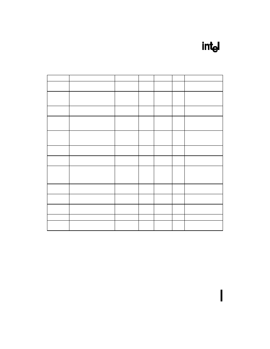
DC CHARACTERISTICS
Table 8. DC Characteristics over Specified Operating Conditions
Symbol
Parameter
Min
Typ (4)
Max
Units
Test Conditions
V
IL
Input Low Voltage
(standard inputs (1))
– 0.5
0.3 V
CC
V
IL1
Input Low Voltage
(RESET#, ports 3, 4, and
5)
– 0.5
0.8
V
IH
Input High Voltage
(standard inputs (1))
0.7 V
CC
V
CC + 0.5
V
IH1
Input High Voltage
(RESET#, ports 3, 4, and
5)
0.2 V
CC + 1.0
V
CC + 0.5
V
OL
Output Low Voltage
(RESET#, ports 1, 2, 5,
P6.6, P6.7, and XTAL2)
0.3
0.45
1.5
V
I
OL = 200 A
I
OL = 3.2 mA
I
OL = 7.0 mA
V
OL1
Output Low Voltage (ports
3, 4)
1.0
V
I
OL = 7 mA
V
OL2
Output Low Voltage
(P6.5:0)
0.45
V
I
OL = 10 mA
V
OH
Output High Voltage
(output pins and I/O
configured as push/pull
outputs)
V
CC – 0.3
V
CC – 0.7
V
CC – 1.5
V
I
OH = – 200 A
I
OH = – 3.2 mA
I
OH = – 7.0 mA
V
TH
+ – VTH–
Hysteresis voltage width
on RESET# pin
0.2
V
I
LI
Input Leakage Current
(standard inputs (1))
± 10
A
V
SS < VIN < VCC – 0.3V
I
LI1
Input Leakage Current
(port 0 – A/D inputs)
± 3A
V
SS < VIN < VREF
I
IH
Input High Current (NMI)
300
A
V
IN = 0.7 VCC
I
IL
Input Low Current (port 2,
except P2.6)
70
A
V
IN = 0.3 VCC
NOTES:
1.
Standard input pins include XTAL1, EA#, and Ports 1 and 2 when configured as inputs.
2.
Maximum current that an external device must sink to ensure test mode entry.
3.
Violating these specifications during reset may cause the device to enter test modes.
4.
Typical values are based on a limited number of samples and are not guaranteed. Operating conditions
for typical values are room temperature and V
REF = VCC = 5.5 V.
5.
Testing is performed down to 8 MHz, although the device is static by design and will typically operate
below 1 Hz.
6.
All voltages are referenced relative to V
SS. When used, VSS refers to the device pin.
7.
Table 9 lists the total current limits during normal (non-transient conditions). The total current listed is the
sum of the pins listed for each specification value.
相关PDF资料 |
PDF描述 |
|---|---|
| S83C51FB-BB44 | 8-BIT, MROM, 24 MHz, MICROCONTROLLER, PQFP44 |
| S83C51FC-5B44 | 8-BIT, MROM, 16 MHz, MICROCONTROLLER, PQFP44 |
| S83C51FC-IA44 | 8-BIT, MROM, 33 MHz, MICROCONTROLLER, PQCC44 |
| S83C51FA-4B44 | 8-BIT, MROM, 16 MHz, MICROCONTROLLER, PQFP44 |
| S83C51FC-AA44 | 8-BIT, MROM, 24 MHz, MICROCONTROLLER, PQCC44 |
相关代理商/技术参数 |
参数描述 |
|---|---|
| S83C198 | 制造商:INTEL 制造商全称:Intel Corporation 功能描述:COMMERCIAL/EXPRESS CHMOS MICROCONTROLLER |
| S83C198-16 | 制造商:未知厂家 制造商全称:未知厂家 功能描述:16-Bit Microcontroller |
| S83C51FA-1 | 制造商:未知厂家 制造商全称:未知厂家 功能描述:8-Bit Microcontroller |
| S83C51FA-24 | 制造商:未知厂家 制造商全称:未知厂家 功能描述:8-Bit Microcontroller |
| S83C51FA-33 | 制造商:未知厂家 制造商全称:未知厂家 功能描述:8-Bit Microcontroller |
发布紧急采购,3分钟左右您将得到回复。