- 您现在的位置:买卖IC网 > PDF目录98071 > S83C196MH (INTEL CORP) 16-BIT, MROM, 16 MHz, MICROCONTROLLER, PQFP80 PDF资料下载
参数资料
| 型号: | S83C196MH |
| 厂商: | INTEL CORP |
| 元件分类: | 微控制器/微处理器 |
| 英文描述: | 16-BIT, MROM, 16 MHz, MICROCONTROLLER, PQFP80 |
| 封装: | SHRINK, QFP-80 |
| 文件页数: | 17/41页 |
| 文件大小: | 1547K |
| 代理商: | S83C196MH |
第1页第2页第3页第4页第5页第6页第7页第8页第9页第10页第11页第12页第13页第14页第15页第16页当前第17页第18页第19页第20页第21页第22页第23页第24页第25页第26页第27页第28页第29页第30页第31页第32页第33页第34页第35页第36页第37页第38页第39页第40页第41页
8XC196MH INDUSTRIAL MOTOR CONTROL CHMOS MICROCONTROLLER
24
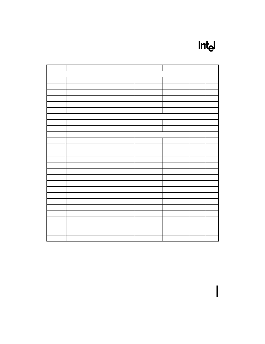
The External Memory System Must Meet These Specifications (Continued)
T
LLGX
BUSWIDTH Hold after ALE/ADV# Low
T
OSC
ns
T
LHDV
ALE/ADV# High to Input Data Valid
3T
OSC – 55
ns
T
AVDV
Address Valid to Input Data Valid
3T
OSC – 55
ns
T
RLDV
RD# Active to Input Data Valid
T
OSC – 30
ns
T
RHDZ
End of RD# to Input Data Float
T
OSC
ns
T
RXDX
Data Hold after RD# Inactive
0
ns
The 8XC196MH will Meet These Specifications
T
XHLH
XTAL1 Rising Edge to ALE Rising
20
110
ns
T
XHLL
XTAL1 Rising Edge to ALE Falling
20
110
ns
T
LHLH
ALE/ADV# Cycle Time
4T
OSC
ns
T
LHLL
ALE/ADV# High Period
T
OSC – 10
T
OSC + 10
ns
T
AVLH
Address Valid to ALE/ADV# High
T
OSC – 17
ns
T
AVLL
Address Valid to ALE/ADV# Low
T
OSC – 17
ns
T
LLAX
Address Hold after ALE/ADV# Low
T
OSC – 40
ns
T
LLRL
ALE/ADV# Low to RD# Low
T
OSC – 30
ns
T
RLRH
RD# Low Period
T
OSC – 5
T
OSC + 25
ns
T
RHLH
RD# High to ALE/ADV# High
T
OSC
T
OSC + 25
ns
T
RLAZ
RD# Low to Address Float
5
ns
T
LLWL
ALE/ADV# Low to WR# Low
T
OSC – 10
ns
T
QVWH
Data Valid before WR# High
T
OSC – 23
ns
T
WLWH
WR# Low Period
T
OSC – 30
ns
T
WHQX
Data Hold after WR# High
T
OSC – 25
ns
T
WHLH
WR# High to ALE/ADV# High
T
OSC – 10
T
OSC + 15
ns
T
WHBX
BHE#, INST Hold after WR# High
T
OSC – 10
ns
T
WHAX
A15:8 Hold after WR# High
T
OSC – 30
ns
T
RHBX
BHE#, INST Hold after RD# High
T
OSC – 10
ns
T
RHAX
A15:8 Hold after RD# High
T
OSC – 30
ns
Table 11. AC Timing Definitions (1) (Continued)
Symbol
Parameter
Min
Max
Units
Notes
NOTES:
1.
Test Conditions: Capacitive load on all pins = 100 pF, rise and fall times = 10 ns, F
OSC = 16 MHz.
2.
Exceeding the maximum specification causes additional wait states.
3.
If wait states are used, add 2T
OSC × n, where n = number of wait states.
4.
Testing is performed down to 8 MHz, although the device is static by design and will typically operate
below 1 Hz.
5.
Assuming back-to-back bus cycles.
6.
8-bit bus only.
相关PDF资料 |
PDF描述 |
|---|---|
| S83C51FB-BB44 | 8-BIT, MROM, 24 MHz, MICROCONTROLLER, PQFP44 |
| S83C51FC-5B44 | 8-BIT, MROM, 16 MHz, MICROCONTROLLER, PQFP44 |
| S83C51FC-IA44 | 8-BIT, MROM, 33 MHz, MICROCONTROLLER, PQCC44 |
| S83C51FA-4B44 | 8-BIT, MROM, 16 MHz, MICROCONTROLLER, PQFP44 |
| S83C51FC-AA44 | 8-BIT, MROM, 24 MHz, MICROCONTROLLER, PQCC44 |
相关代理商/技术参数 |
参数描述 |
|---|---|
| S83C198 | 制造商:INTEL 制造商全称:Intel Corporation 功能描述:COMMERCIAL/EXPRESS CHMOS MICROCONTROLLER |
| S83C198-16 | 制造商:未知厂家 制造商全称:未知厂家 功能描述:16-Bit Microcontroller |
| S83C51FA-1 | 制造商:未知厂家 制造商全称:未知厂家 功能描述:8-Bit Microcontroller |
| S83C51FA-24 | 制造商:未知厂家 制造商全称:未知厂家 功能描述:8-Bit Microcontroller |
| S83C51FA-33 | 制造商:未知厂家 制造商全称:未知厂家 功能描述:8-Bit Microcontroller |
发布紧急采购,3分钟左右您将得到回复。