- 您现在的位置:买卖IC网 > Datasheet目录508 > SI1557DH-T1-E3 (Vishay Siliconix)MOSFET N/P-CH 12V SC70-6 Datasheet资料下载
参数资料
| 型号: | SI1557DH-T1-E3 |
| 厂商: | Vishay Siliconix |
| 文件页数: | 10/14页 |
| 文件大小: | 0K |
| 描述: | MOSFET N/P-CH 12V SC70-6 |
| 标准包装: | 3,000 |
| 系列: | TrenchFET® |
| FET 型: | N 和 P 沟道 |
| FET 特点: | 逻辑电平门 |
| 漏极至源极电压(Vdss): | 12V |
| 电流 - 连续漏极(Id) @ 25° C: | 1.2A,770mA |
| 开态Rds(最大)@ Id, Vgs @ 25° C: | 235 毫欧 @ 1.2A,4.5V |
| Id 时的 Vgs(th)(最大): | 450mV @ 100µA |
| 闸电荷(Qg) @ Vgs: | 1.2nC @ 4.5V |
| 功率 - 最大: | 470mW |
| 安装类型: | * |
| 封装/外壳: | 6-TSSOP,SC-88,SOT-363 |
| 供应商设备封装: | SC-70-6 |
| 包装: | 带卷 (TR) |
�� �
�
�AN816�
�Vishay� Siliconix�
�Dual-Channel� LITTLE� FOOT� R� 6-Pin� SC-70� MOSFET�
�Copper� Leadframe� Version�
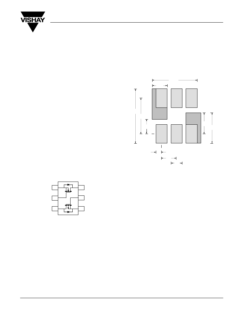
�Recommended� Pad� Pattern� and� Thermal� Performance�
�INTRODUCTION�
�26� (mil)�
�87� (mil)�
�The� new� dual� 6-pin� SC-70� package� with� a� copper� leadframe�
�enables� improved� on-resistance� values� and� enhanced�
�thermal� performance� as� compared� to� the� existing� 3-pin� and�
�6-pin� packages� with� Alloy� 42� leadframes.� These� devices� are�
�intended� for� small� to� medium� load� applications� where� a�
�miniaturized� package� is� required.� Devices� in� this� package�
�come� in� a� range� of� on-resistance� values,� in� n-channel� and�
�p-channel� versions.� This� technical� note� discusses� pin-outs,�
�package� outlines,� pad� patterns,� evaluation� board� layout,� and�
�thermal� performance� for� the� dual-channel� version.�
�96� (mil)�
�71� (mil)�
�23� (mil)�
�6�
�5�
�4�
�48� (mil)�
�61� (mil)�
�PIN-OUT�
�0.0� (mil)�
�1�
�2�
�3�
�Figure� 1� shows� the� pin-out� description� and� Pin� 1� identification�
�for� the� dual-channel� SC-70� device� in� the� 6-pin� configuration.�
�Both� n-and� p-channel� devices� are� available� in� this� package� –�
�the� drawing� example� below� illustrates� the� p-channel� device.�
�8� (mil)�
�26� (mil)�
�16� (mil)�
�SOT-363�
�SC-70� (6-LEADS)�
�FIGURE� 2.�
�SC-70� (6� leads)� Dual�
�S� 1�
�G� 1�
�1�
�2�
�6�
�5�
�D� 1�
�G� 2�
�EVALUATION� BOARD� FOR� THE� DUAL-�
�CHANNEL� SC70-6�
�D� 2�
�3�
�Top� View�
�FIGURE� 1.�
�4�
�S� 2�
�The� 6-pin� SC-70� evaluation� board� (EVB)� shown� in� Figure� 3�
�measures� 0.6� in.� by� 0.5� in.� The� copper� pad� traces� are� the� same�
�as� described� in� the� previous� section,� Basic� Pad� Patterns� .� The�
�board� allows� for� examination� from� the� outer� pins� to� the� 6-pin�
�DIP� connections,� permitting� test� sockets� to� be� used� in�
�evaluation� testing.�
�For� package� dimensions� see� outline� drawing� SC-70� (6-Leads)�
�(� http://www.vishay.com/doc?71154� )�
�BASIC� PAD� PATTERNS�
�See� Application� Note� 826,� Recommended� Minimum� Pad�
�Patterns� With� Outline� Drawing� Access� for� Vishay� Siliconix�
�MOSFET� s,� (� http://www.vishay.com/doc?72286� )� for� the� SC-70�
�6-pin� basic� pad� layout� and� dimensions.� This� pad� pattern� is�
�sufficient� for� the� low-power� applications� for� which� this� package�
�is� intended.� Increasing� the� drain� pad� pattern� (Figure� 2)� yields�
�a� reduction� in� thermal� resistance� and� is� a� preferred� footprint.�
�Document� Number:� 71405�
�12-Dec-03�
�The� thermal� performance� of� the� dual� 6-pin� SC-70� has� been�
�measured� on� the� EVB,� comparing� both� the� copper� and� Alloy�
�42� leadframes.� This� test� was� then� repeated� using� the� 1-inch� 2�
�PCB� with� dual-side� copper� coating.�
�A� helpful� way� of� displaying� the� thermal� performance� of� the�
�6-pin� SC-70� dual� copper� leadframe� is� to� compare� it� to� the�
�traditional� Alloy� 42� version.�
�www.vishay.com�
�1�
�相关PDF资料 |
PDF描述 |
|---|---|
| SI1563EDH-T1-GE3 | MOSFET N/P-CH 20V SC70-6 |
| SI1900DL-T1-E3 | MOSFET N-CH DUAL 30V SC70-6 |
| SI1902DL-T1-GE3 | MOSFET N-CH G-S 20V DUAL SC-70-6 |
| SI1926DL-T1-E3 | MOSF N CH DUAL D-S 60V SC-70-6 |
| SI1967DH-T1-E3 | MOSFET 2P-CH 20V 1.3A SC70-6 |
相关代理商/技术参数 |
参数描述 |
|---|---|
| SI1563DH | 制造商:VISHAY 制造商全称:Vishay Siliconix 功能描述:Complementary 20-V (D-S) Low-Threshold MOSFET |
| SI1563DH_08 | 制造商:VISHAY 制造商全称:Vishay Siliconix 功能描述:Complementary 20-V (D-S) Low-Threshold MOSFET |
| SI1563DH_10 | 制造商:VISHAY 制造商全称:Vishay Siliconix 功能描述:Complementary 20 V (D-S) Low-Threshold MOSFET |
| SI1563DH-T1 | 功能描述:MOSFET 20V 1.28/1.0A 0.48W RoHS:否 制造商:STMicroelectronics 晶体管极性:N-Channel 汲极/源极击穿电压:650 V 闸/源击穿电压:25 V 漏极连续电流:130 A 电阻汲极/源极 RDS(导通):0.014 Ohms 配置:Single 最大工作温度: 安装风格:Through Hole 封装 / 箱体:Max247 封装:Tube |
| SI1563DH-T1-E3 | 功能描述:MOSFET 20V 1.28/1.0A 16 RoHS:否 制造商:STMicroelectronics 晶体管极性:N-Channel 汲极/源极击穿电压:650 V 闸/源击穿电压:25 V 漏极连续电流:130 A 电阻汲极/源极 RDS(导通):0.014 Ohms 配置:Single 最大工作温度: 安装风格:Through Hole 封装 / 箱体:Max247 封装:Tube |
发布紧急采购,3分钟左右您将得到回复。