- 您现在的位置:买卖IC网 > Datasheet目录510 > SI4622DY-T1-E3 (Vishay Siliconix)MOSFET N-CH D-S 30V 8-SOIC Datasheet资料下载
参数资料
| 型号: | SI4622DY-T1-E3 |
| 厂商: | Vishay Siliconix |
| 文件页数: | 13/15页 |
| 文件大小: | 0K |
| 描述: | MOSFET N-CH D-S 30V 8-SOIC |
| 标准包装: | 2,500 |
| 系列: | SkyFET®, TrenchFET® |
| FET 型: | 2 个 N 沟道(双) |
| FET 特点: | 标准 |
| 漏极至源极电压(Vdss): | 30V |
| 电流 - 连续漏极(Id) @ 25° C: | 8A |
| 开态Rds(最大)@ Id, Vgs @ 25° C: | 16 毫欧 @ 9.6A,10V |
| Id 时的 Vgs(th)(最大): | 2.5V @ 1mA |
| 闸电荷(Qg) @ Vgs: | 60nC @ 10V |
| 输入电容 (Ciss) @ Vds: | 2458pF @ 15V |
| 功率 - 最大: | 3.3W,3.1W |
| 安装类型: | 表面贴装 |
| 封装/外壳: | 8-SOIC(0.154",3.90mm 宽) |
| 供应商设备封装: | 8-SOICN |
| 包装: | 带卷 (TR) |
�� �
�
�VISHAY� SILICONIX�
�TrenchFET� ?� Power� MOSFETs�
�Application� Note� 808�
�Mounting� LITTLE� FOOT� ?� ,� SO-8� Power� MOSFETs�
�Wharton� McDaniel�
�0.2� 88�
�Surface-mounted� LITTLE� FOOT� power� MOSFETs� use�
�integrated� circuit� and� small-signal� packages� which� have�
�7.3�
�been� been� modified� to� provide� the� heat� transfer� capabilities�
�required� by� power� devices.� Leadframe� materials� and�
�design,� molding� compounds,� and� die� attach� materials� have�
�been� changed,� while� the� footprint� of� the� packages� remains�
�the� same.�
�See� Application� Note� 826,� Recommended� Minimum� Pad�
�Patterns� With� Outline� Drawing� Access� for� Vishay� Siliconix�
�0.050�
�1.27�
�0.027�
�0.69�
�0.07� 8�
�1.9� 8�
�0.2�
�5.07�
�0.0� 88�
�2.25�
�0.0� 88�
�2.25�
�MOSFETs,� (� http://www.vishay.com/ppg?72286� ),� for� the�
�basis� of� the� pad� design� for� a� LITTLE� FOOT� SO-8� power�
�MOSFET.� In� converting� this� recommended� minimum� pad�
�to� the� pad� set� for� a� power� MOSFET,� designers� must� make�
�two� connections:� an� electrical� connection� and� a� thermal�
�connection,� to� draw� heat� away� from� the� package.�
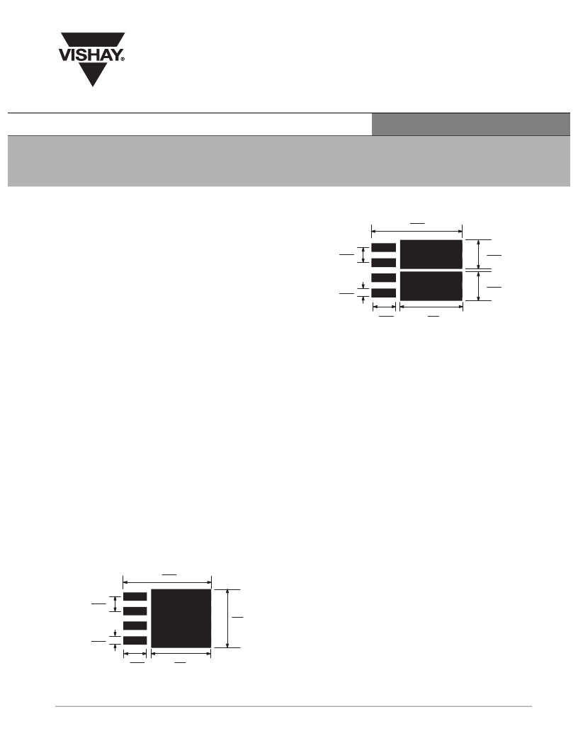
�In� the� case� of� the� SO-8� package,� the� thermal� connections�
�are� very� simple.� Pins� 5,� 6,� 7,� and� 8� are� the� drain� of� the�
�MOSFET� for� a� single� MOSFET� package� and� are� connected�
�together.� In� a� dual� package,� pins� 5� and� 6� are� one� drain,� and�
�pins� 7� and� 8� are� the� other� drain.� For� a� small-signal� device� or�
�integrated� circuit,� typical� connections� would� be� made� with�
�traces� that� are� 0.020� inches� wide.� Since� the� drain� pins� serve�
�the� additional� function� of� providing� the� thermal� connection�
�to� the� package,� this� level� of� connection� is� inadequate.� The�
�total� cross� section� of� the� copper� may� be� adequate� to� carry�
�the� current� required� for� the� application,� but� it� presents� a�
�large� thermal� impedance.� Also,� heat� spreads� in� a� circular�
�fashion� from� the� heat� source.� In� this� case� the� drain� pins� are�
�the� heat� sources� when� looking� at� heat� spread� on� the� PC�
�board.�
�0.2� 88�
�7.3�
�0.050�
�1.27�
�0.196�
�5.0�
�0.027�
�0.69�
�Figure� 2.� Dual� MOSFET� SO-8� Pad� Pattern�
�With� Copper� Spreading�
�The� minimum� recommended� pad� patterns� for� the�
�single-MOSFET� SO-8� with� copper� spreading� (Figure� 1)� and�
�dual-MOSFET� SO-8� with� copper� spreading� (Figure� 2)� show�
�the� starting� point� for� utilizing� the� board� area� available� for� the�
�heat-spreading� copper.� To� create� this� pattern,� a� plane� of�
�copper� overlies� the� drain� pins.� The� copper� plane� connects�
�the� drain� pins� electrically,� but� more� importantly� provides�
�planar� copper� to� draw� heat� from� the� drain� leads� and� start� the�
�process� of� spreading� the� heat� so� it� can� be� dissipated� into� the�
�ambient� air.� These� patterns� use� all� the� available� area�
�underneath� the� body� for� this� purpose.�
�Since� surface-mounted� packages� are� small,� and� reflow�
�soldering� is� the� most� common� way� in� which� these� are�
�affixed� to� the� PC� board,� “thermal”� connections� from� the�
�planar� copper� to� the� pads� have� not� been� used.� Even� if�
�additional� planar� copper� area� is� used,� there� should� be� no�
�problems� in� the� soldering� process.� The� actual� solder�
�connections� are� defined� by� the� solder� mask� openings.� By�
�combining� the� basic� footprint� with� the� copper� plane� on� the�
�drain� pins,� the� solder� mask� generation� occurs� automatically.�
�A� final� item� to� keep� in� mind� is� the� width� of� the� power� traces.�
�The� absolute� minimum� power� trace� width� must� be�
�determined� by� the� amount� of� current� it� has� to� carry.� For�
�0.07� 8�
�1.9� 8�
�0.2�
�5.07�
�thermal� reasons,� this� minimum� width� should� be� at� least�
�0.020� inches.� The� use� of� wide� traces� connected� to� the� drain�
�Figure� 1.� Single� MOSFET� SO-8� Pad�
�Pattern� With� Copper� Spreading�
�Document� Number:� 70740�
�Revision:� 18-Jun-07�
�plane� provides� a� low� impedance� path� for� heat� to� move� away�
�from� the� device.�
�www.vishay.com�
�1�
�相关PDF资料 |
PDF描述 |
|---|---|
| SI4632DY-T1-GE3 | MOSFET N-CH 25V 8-SOIC |
| SI4634DY-T1-E3 | MOSFET N-CH D-S 30V 8-SOIC |
| SI4636DY-T1-E3 | MOSFET N-CH/SCHOTTKY 30V 8SOIC |
| SI4638DY-T1-E3 | MOSFET N-CH/SCHOTTKY 30V 8SOIC |
| SI4646DY-T1-GE3 | MOSFET N-CH/SCHOTTKY 30V 8SOIC |
相关代理商/技术参数 |
参数描述 |
|---|---|
| SI4622DY-T1-GE3 | 功能描述:MOSFET 30V 8.0A 3.3/3.1W 16/26.4mohm @ 10V RoHS:否 制造商:STMicroelectronics 晶体管极性:N-Channel 汲极/源极击穿电压:650 V 闸/源击穿电压:25 V 漏极连续电流:130 A 电阻汲极/源极 RDS(导通):0.014 Ohms 配置:Single 最大工作温度: 安装风格:Through Hole 封装 / 箱体:Max247 封装:Tube |
| SI4626ADY-T1-E3 | 功能描述:MOSFET 30V 30A 6.0W 3.3mohm @ 10V RoHS:否 制造商:STMicroelectronics 晶体管极性:N-Channel 汲极/源极击穿电压:650 V 闸/源击穿电压:25 V 漏极连续电流:130 A 电阻汲极/源极 RDS(导通):0.014 Ohms 配置:Single 最大工作温度: 安装风格:Through Hole 封装 / 箱体:Max247 封装:Tube |
| SI4626ADY-T1-GE3 | 功能描述:MOSFET 30V 30A 6.0W 3.3mohm @ 10V RoHS:否 制造商:STMicroelectronics 晶体管极性:N-Channel 汲极/源极击穿电压:650 V 闸/源击穿电压:25 V 漏极连续电流:130 A 电阻汲极/源极 RDS(导通):0.014 Ohms 配置:Single 最大工作温度: 安装风格:Through Hole 封装 / 箱体:Max247 封装:Tube |
| SI4626DY-T1-E3 | 功能描述:MOSFET 30V 30A 6.0W RoHS:否 制造商:STMicroelectronics 晶体管极性:N-Channel 汲极/源极击穿电压:650 V 闸/源击穿电压:25 V 漏极连续电流:130 A 电阻汲极/源极 RDS(导通):0.014 Ohms 配置:Single 最大工作温度: 安装风格:Through Hole 封装 / 箱体:Max247 封装:Tube |
| SI4628DY | 制造商:VISHAY 制造商全称:Vishay Siliconix 功能描述:N-Channel 30-V (D-S) MOSFET with Schottky Diode |
发布紧急采购,3分钟左右您将得到回复。