- 您现在的位置:买卖IC网 > PDF目录9578 > SI5315A-C-GMR (Silicon Laboratories Inc)IC CLK MULT 8KHZ-644.53MHZ 36QFN PDF资料下载
参数资料
| 型号: | SI5315A-C-GMR |
| 厂商: | Silicon Laboratories Inc |
| 文件页数: | 25/54页 |
| 文件大小: | 0K |
| 描述: | IC CLK MULT 8KHZ-644.53MHZ 36QFN |
| 应用说明: | SI5315/17 Crystal Selection AppNote |
| 标准包装: | 250 |
| 系列: | DSPLL® |
| 类型: | 时钟/频率倍增器,抖动衰减器,多路复用器 |
| PLL: | 无 |
| 主要目的: | 以太网,SONET/SDH/PDH,电信 |
| 输入: | CML,CMOS,LVDS,LVPECL |
| 输出: | CML,CMOS,LVDS,LVPECL |
| 电路数: | 1 |
| 比率 - 输入:输出: | 2:2 |
| 差分 - 输入:输出: | 是/是 |
| 频率 - 最大: | 644.53MHz |
| 电源电压: | 1.71 V ~ 3.63 V |
| 工作温度: | -40°C ~ 85°C |
| 安装类型: | 表面贴装 |
| 封装/外壳: | 36-VFQFN 裸露焊盘 |
| 供应商设备封装: | 36-QFN(6x6) |
| 包装: | 带卷 (TR) |
第1页第2页第3页第4页第5页第6页第7页第8页第9页第10页第11页第12页第13页第14页第15页第16页第17页第18页第19页第20页第21页第22页第23页第24页当前第25页第26页第27页第28页第29页第30页第31页第32页第33页第34页第35页第36页第37页第38页第39页第40页第41页第42页第43页第44页第45页第46页第47页第48页第49页第50页第51页第52页第53页第54页
Si5315
Rev. 1.0
31
The prioritization of clock inputs for automatic switching is shown in Table 14. This priority is hardwired in the
devices.
At power-on or reset, the valid CKINn with the highest priority (1 being the highest priority) is automatically
selected. If no valid CKINn is available, the device suppresses the output clocks and waits for a valid CKINn signal.
If the currently selected CKINn goes into an alarm state, the next valid CKINn in priority order is selected. If no valid
CKINn is available, the device enters holdover.
Operation in revertive and non- revertive is different when a signal becomes valid:
Revertive (AUTOSEL = H):
The device constantly monitors all CKINn. If a CKINn with a higher priority than
the current active CKINn becomes valid, the active CKINn is changed to the
CKINn with the highest priority.
Non-revertive (AUTOSEL = M): The active clock does not change until there is an alarm on the active clock. The
device will then select the highest priority CKINn that is valid. Once in holdover,
the device will switch to the first CKINn that becomes valid.
5.4. Alarms
Summary alarms are available to indicate the overall status of the input signals. Alarm outputs stay high until all the
alarm conditions for that alarm output are cleared.
5.4.1. Loss-of-Signal
The device has loss-of-signal circuitry that continuously monitors CKINn for missing pulses. The LOS circuitry
generates an internal LOSn_INT output signal that is processed with other alarms to generate LOS1 and LOS2.
An LOS condition on CKIN1 causes the internal LOS1_INT alarm to become active. Similarly, an LOS condition on
CKINn causes the LOSn_INT alarm to become active. Once a LOSn_INT alarm is asserted on one of the input
clocks, it remains asserted until that input clock is validated over a designated time period. The time to clear
LOSn_INT after a valid input clock appears is listed in Table 3, “AC Characteristics”. If another error condition on
the same input clock is detected during the validation time then the alarm remains asserted and the validation time
starts over.
5.4.1.1. LOS Algorithm
The LOS circuitry divides down each input clock to produce an 8 kHz to 2 MHz signal. The LOS circuitry over
samples this divided down input clock using a 40 MHz clock to search for extended periods of time without input
clock transitions. If the LOS monitor detects twice the normal number of samples without a clock edge, a
LOSn_INT alarm is declared. Table 3, “AC Characteristics” gives the minimum and maximum amount of time for
the LOS monitor to trigger.
5.4.1.2. Lock Detect
The PLL lock detection algorithm indicates the lock status on the LOL output pin. The algorithm works by
continuously monitoring the phase of the input clock in relation to the phase of the feedback clock. If the time
between two consecutive phase cycle slips is greater than the retrigger time, the PLL is in lock. The LOL output
has a guaranteed minimum pulse width as shown in (Table 3, “AC Characteristics”). The LOL pin is also held in the
active state during an internal PLL calibration. The retrigger time is automatically set based on the PLL closed loop
bandwidth (See Table 15).
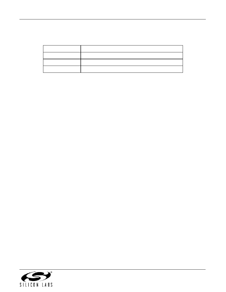
Table 14. Input Clock Priority for Auto Switching
Priority
Input Clocks
1CKIN1
2CKIN2
3
Holdover
相关PDF资料 |
PDF描述 |
|---|---|
| VE-2NT-MY-S | CONVERTER MOD DC/DC 6.5V 50W |
| VE-B3W-IU | CONVERTER MOD DC/DC 5.5V 200W |
| VE-B3T-IU | CONVERTER MOD DC/DC 6.5V 200W |
| VE-2NR-MY-S | CONVERTER MOD DC/DC 7.5V 50W |
| VE-B3P-IU | CONVERTER MOD DC/DC 13.8V 200W |
相关代理商/技术参数 |
参数描述 |
|---|---|
| Si5315B-C-GM | 功能描述:时钟发生器及支持产品 Pin-Prgrmmbl SyncE Clck Mlt/Jttr Attntr RoHS:否 制造商:Silicon Labs 类型:Clock Generators 最大输入频率:14.318 MHz 最大输出频率:166 MHz 输出端数量:16 占空比 - 最大:55 % 工作电源电压:3.3 V 工作电源电流:1 mA 最大工作温度:+ 85 C 安装风格:SMD/SMT 封装 / 箱体:QFN-56 |
| SI5315B-C-GMR | 功能描述:时钟发生器及支持产品 Pin-Ctrl SyncE Clk Xplier/Jitt Attn 2/2 RoHS:否 制造商:Silicon Labs 类型:Clock Generators 最大输入频率:14.318 MHz 最大输出频率:166 MHz 输出端数量:16 占空比 - 最大:55 % 工作电源电压:3.3 V 工作电源电流:1 mA 最大工作温度:+ 85 C 安装风格:SMD/SMT 封装 / 箱体:QFN-56 |
| SI5315-C | 制造商:AUK 制造商全称:AUK corp 功能描述:IRED |
| SI5315-C(B) | 制造商:AUK 制造商全称:AUK corp 功能描述:IRED |
| SI5315-C_1 | 制造商:AUK 制造商全称:AUK corp 功能描述:IRED |
发布紧急采购,3分钟左右您将得到回复。