- 您现在的位置:买卖IC网 > PDF目录9578 > SI5315A-C-GMR (Silicon Laboratories Inc)IC CLK MULT 8KHZ-644.53MHZ 36QFN PDF资料下载
参数资料
| 型号: | SI5315A-C-GMR |
| 厂商: | Silicon Laboratories Inc |
| 文件页数: | 39/54页 |
| 文件大小: | 0K |
| 描述: | IC CLK MULT 8KHZ-644.53MHZ 36QFN |
| 应用说明: | SI5315/17 Crystal Selection AppNote |
| 标准包装: | 250 |
| 系列: | DSPLL® |
| 类型: | 时钟/频率倍增器,抖动衰减器,多路复用器 |
| PLL: | 无 |
| 主要目的: | 以太网,SONET/SDH/PDH,电信 |
| 输入: | CML,CMOS,LVDS,LVPECL |
| 输出: | CML,CMOS,LVDS,LVPECL |
| 电路数: | 1 |
| 比率 - 输入:输出: | 2:2 |
| 差分 - 输入:输出: | 是/是 |
| 频率 - 最大: | 644.53MHz |
| 电源电压: | 1.71 V ~ 3.63 V |
| 工作温度: | -40°C ~ 85°C |
| 安装类型: | 表面贴装 |
| 封装/外壳: | 36-VFQFN 裸露焊盘 |
| 供应商设备封装: | 36-QFN(6x6) |
| 包装: | 带卷 (TR) |
第1页第2页第3页第4页第5页第6页第7页第8页第9页第10页第11页第12页第13页第14页第15页第16页第17页第18页第19页第20页第21页第22页第23页第24页第25页第26页第27页第28页第29页第30页第31页第32页第33页第34页第35页第36页第37页第38页当前第39页第40页第41页第42页第43页第44页第45页第46页第47页第48页第49页第50页第51页第52页第53页第54页
Si5315
44
Rev. 1.0
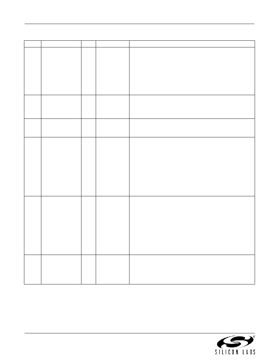
5, 10,
32
VDD
Supply
Supply.
The device operates from a 1.8, 2.5, or 3.3 V supply. Bypass
capacitors should be associated with the following VDD pins:
5
0.1 F
10
0.1 F
32
0.1 F
A 1.0 F should also be placed as close to device as is prac-
tical.
7
6
XB
XA
IAnalog
External Crystal or Reference Clock.
External crystal should be connected to these pins to use
internal oscillator based reference. Crystal or reference clock
selection is set by the XTAL/CLOCK pin.
8,
15,19,
20,31
GND
Supply
Ground.
Must be connected to system ground. Minimize the ground
path impedance for optimal performance of this device.
9
AUTOSEL
I
3-Level
Manual/Automatic Clock Selection.
Three level input that selects the method of input clock selec-
tion to be used.
L = Manual
M = Automatic non-revertive
H = Automatic revertive
This pin has a weak pull-up and weak pull-down and defaults
to M.
Some designs may require an external resistor voltage
divider when driven by an active device that will tri-state.
11
XTAL/CLOCK
I
3-Level
External Crystal or Reference Clock Rate.
Three level input that selects the type and rate of external
crystal or reference clock to be applied to the XA/XB port.
This pin has both a weak pull-up and a weak pull-down and
defaults to M.
L = Crystal
M = Clock (Default)
H = Reserved
Some designs may require an external resistor voltage
divider when driven by an active device that will tri-state.
12
13
CKIN2+
CKIN2–
I
Clock Input 2.
Differential input clock. This input can also be driven with a
single-ended signal. Input frequency selected from a table of
values. The same frequency must be applied to CKIN1 and
CKIN2.
Table 19. Si5315 Pin Descriptions (Continued)
Pin #
Pin Name
I/O
Signal Level
Description
相关PDF资料 |
PDF描述 |
|---|---|
| VE-2NT-MY-S | CONVERTER MOD DC/DC 6.5V 50W |
| VE-B3W-IU | CONVERTER MOD DC/DC 5.5V 200W |
| VE-B3T-IU | CONVERTER MOD DC/DC 6.5V 200W |
| VE-2NR-MY-S | CONVERTER MOD DC/DC 7.5V 50W |
| VE-B3P-IU | CONVERTER MOD DC/DC 13.8V 200W |
相关代理商/技术参数 |
参数描述 |
|---|---|
| Si5315B-C-GM | 功能描述:时钟发生器及支持产品 Pin-Prgrmmbl SyncE Clck Mlt/Jttr Attntr RoHS:否 制造商:Silicon Labs 类型:Clock Generators 最大输入频率:14.318 MHz 最大输出频率:166 MHz 输出端数量:16 占空比 - 最大:55 % 工作电源电压:3.3 V 工作电源电流:1 mA 最大工作温度:+ 85 C 安装风格:SMD/SMT 封装 / 箱体:QFN-56 |
| SI5315B-C-GMR | 功能描述:时钟发生器及支持产品 Pin-Ctrl SyncE Clk Xplier/Jitt Attn 2/2 RoHS:否 制造商:Silicon Labs 类型:Clock Generators 最大输入频率:14.318 MHz 最大输出频率:166 MHz 输出端数量:16 占空比 - 最大:55 % 工作电源电压:3.3 V 工作电源电流:1 mA 最大工作温度:+ 85 C 安装风格:SMD/SMT 封装 / 箱体:QFN-56 |
| SI5315-C | 制造商:AUK 制造商全称:AUK corp 功能描述:IRED |
| SI5315-C(B) | 制造商:AUK 制造商全称:AUK corp 功能描述:IRED |
| SI5315-C_1 | 制造商:AUK 制造商全称:AUK corp 功能描述:IRED |
发布紧急采购,3分钟左右您将得到回复。