- 您现在的位置:买卖IC网 > PDF目录8983 > SI5338Q-A-GM (Silicon Laboratories Inc)IC CLK GEN I2C BUS PROG 24QFN PDF资料下载
参数资料
| 型号: | SI5338Q-A-GM |
| 厂商: | Silicon Laboratories Inc |
| 文件页数: | 27/44页 |
| 文件大小: | 0K |
| 描述: | IC CLK GEN I2C BUS PROG 24QFN |
| 标准包装: | 490 |
| 系列: | MultiSynth™ |
| 类型: | * |
| PLL: | 是 |
| 输入: | CML,HCSL,HSCL,LVDS,LVPECL,晶体 |
| 输出: | CMOS,HCSL. HSTL. LVDS. LVPECL. SSTL |
| 电路数: | 1 |
| 比率 - 输入:输出: | 2:4 |
| 差分 - 输入:输出: | 是/是 |
| 频率 - 最大: | 200MHz |
| 除法器/乘法器: | 是/是 |
| 电源电压: | 1.71 V ~ 3.63 V |
| 工作温度: | -40°C ~ 85°C |
| 安装类型: | 表面贴装 |
| 封装/外壳: | 24-VFQFN 裸露焊盘 |
| 供应商设备封装: | 24-QFN(4x4) |
| 包装: | 托盘 |
第1页第2页第3页第4页第5页第6页第7页第8页第9页第10页第11页第12页第13页第14页第15页第16页第17页第18页第19页第20页第21页第22页第23页第24页第25页第26页当前第27页第28页第29页第30页第31页第32页第33页第34页第35页第36页第37页第38页第39页第40页第41页第42页第43页第44页
Si5338
Rev. 1.3
33
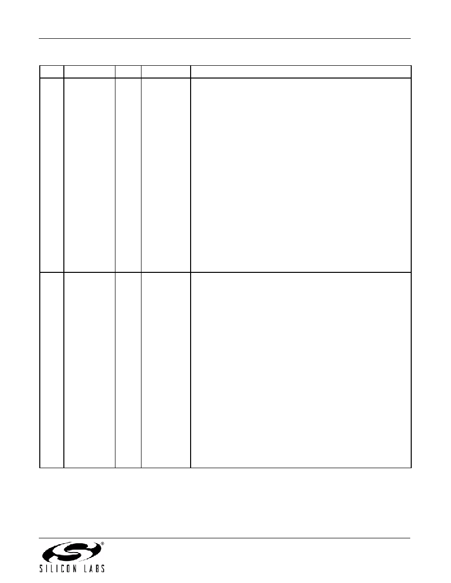
3IN3
I
Multi
This pin can have one of the following functions depending on the
part number:
CLKIN (for Si5338A/B/C and Si5338N/P/Q devices only)
Provides a high-impedance clock input for single ended clock
signals. This input should be dc-coupled as shown in “3.2. Input
If this pin is not used, it should be connected to ground.
PINC (for Si5338D/E/F devices only)
Used as the phase increment pin. See "3.10.2. Output Phase
Increment/Decrement" on page 26 for more details. Minimum
pulse width of 100 ns is required for proper operation. If this pin is
not used, it should be connected to ground.
FINC (for Si5338G/H/J devices only)
Used as the frequency increment pin. See "3.10.1. Frequency
Increment/Decrement" on page 26 for more details. Minimum
pulse width of 100 ns is required for proper operation. If this pin is
not used, it should be connected to ground.
OEB (for Si5338K/L/M devices only)
Used as an output enable pin. 0 = All outputs enabled; 1 = All
outputs disabled. By default, outputs are tri-stated when disabled.
4IN4
I
Multi
This pin can have one of the following functions depending on the
part number
I2C_LSB (for Si5338A/B/C and Si5338K/L/M devices only)
This is the LSB of the Si5338 I2C address. 0 = I2C address
70h (111 0000), 1 = I2C address 71h (111 0001).
FDBK (for Si5338N/P/Q devices only)
Provides a high-impedance feedback input for single-ended clock
signals. This input should be dc-coupled as shown in “3.2. Input
Stage”, Figure 3. If this pin is not used, it should be connected to
ground.
PDEC (for Si5338D/E/F) devices only)
Used as the phase decrement pin. See “3.10.2. Output Phase
Increment/Decrement” for more details. Minimum pulse width of
100 ns is required for proper operation. If this pin is not used, it
should be connected to ground.
FDEC (for Si5338G/H/J devices only)
Used as the frequency decrement pin. See “3.10.1. Frequency
Increment/Decrement” for more details. Minimum pulse width of
100 ns is required for proper operation. If this pin is not used, it
should be connected to ground.
Table 16. Si5338 Pin Descriptions (Continued)
Pin #
Pin Name
I/O
Signal Type
Description
相关PDF资料 |
PDF描述 |
|---|---|
| AD5323BRUZ | IC DAC 12BIT DUAL R-R 16-TSSOP |
| SI5338M-A-GM | IC CLK GEN I2C BUS PROG 24QFN |
| AD5453YRMZ | IC DAC 14BIT MULTIPLYING 8-MSOP |
| ICS843156AKILFT | IC CLK GENERATOR 32VFQFP |
| VI-B0P-MY-F4 | CONVERTER MOD DC/DC 13.8V 50W |
相关代理商/技术参数 |
参数描述 |
|---|---|
| SI5338Q-A-GMR | 功能描述:时钟发生器及支持产品 I2C Program Clk Gen 0.16-200MHz 4Clk In RoHS:否 制造商:Silicon Labs 类型:Clock Generators 最大输入频率:14.318 MHz 最大输出频率:166 MHz 输出端数量:16 占空比 - 最大:55 % 工作电源电压:3.3 V 工作电源电流:1 mA 最大工作温度:+ 85 C 安装风格:SMD/SMT 封装 / 箱体:QFN-56 |
| Si5338Q-Axxxxx-GM | 制造商:Silicon Laboratories Inc 功能描述: |
| SI5338Q-B02153-GM | 制造商:Silicon Laboratories Inc 功能描述: 制造商:Silicon Laboratories Inc 功能描述:IC CLK GEN I2C BUS PROG 24QFN |
| Si5338Q-B-GM | 功能描述:时钟发生器及支持产品 I2C-prgrmmbl clock generatr .16-200 MHz RoHS:否 制造商:Silicon Labs 类型:Clock Generators 最大输入频率:14.318 MHz 最大输出频率:166 MHz 输出端数量:16 占空比 - 最大:55 % 工作电源电压:3.3 V 工作电源电流:1 mA 最大工作温度:+ 85 C 安装风格:SMD/SMT 封装 / 箱体:QFN-56 |
| Si5338Q-B-GMR | 功能描述:时钟发生器及支持产品 I2C Program Clk Gen 0.16-200MHz 4Clk In RoHS:否 制造商:Silicon Labs 类型:Clock Generators 最大输入频率:14.318 MHz 最大输出频率:166 MHz 输出端数量:16 占空比 - 最大:55 % 工作电源电压:3.3 V 工作电源电流:1 mA 最大工作温度:+ 85 C 安装风格:SMD/SMT 封装 / 箱体:QFN-56 |
发布紧急采购,3分钟左右您将得到回复。