- 您现在的位置:买卖IC网 > PDF目录8983 > SI5338Q-A-GM (Silicon Laboratories Inc)IC CLK GEN I2C BUS PROG 24QFN PDF资料下载
参数资料
| 型号: | SI5338Q-A-GM |
| 厂商: | Silicon Laboratories Inc |
| 文件页数: | 28/44页 |
| 文件大小: | 0K |
| 描述: | IC CLK GEN I2C BUS PROG 24QFN |
| 标准包装: | 490 |
| 系列: | MultiSynth™ |
| 类型: | * |
| PLL: | 是 |
| 输入: | CML,HCSL,HSCL,LVDS,LVPECL,晶体 |
| 输出: | CMOS,HCSL. HSTL. LVDS. LVPECL. SSTL |
| 电路数: | 1 |
| 比率 - 输入:输出: | 2:4 |
| 差分 - 输入:输出: | 是/是 |
| 频率 - 最大: | 200MHz |
| 除法器/乘法器: | 是/是 |
| 电源电压: | 1.71 V ~ 3.63 V |
| 工作温度: | -40°C ~ 85°C |
| 安装类型: | 表面贴装 |
| 封装/外壳: | 24-VFQFN 裸露焊盘 |
| 供应商设备封装: | 24-QFN(4x4) |
| 包装: | 托盘 |
第1页第2页第3页第4页第5页第6页第7页第8页第9页第10页第11页第12页第13页第14页第15页第16页第17页第18页第19页第20页第21页第22页第23页第24页第25页第26页第27页当前第28页第29页第30页第31页第32页第33页第34页第35页第36页第37页第38页第39页第40页第41页第42页第43页第44页
Si5338
34
Rev. 1.3
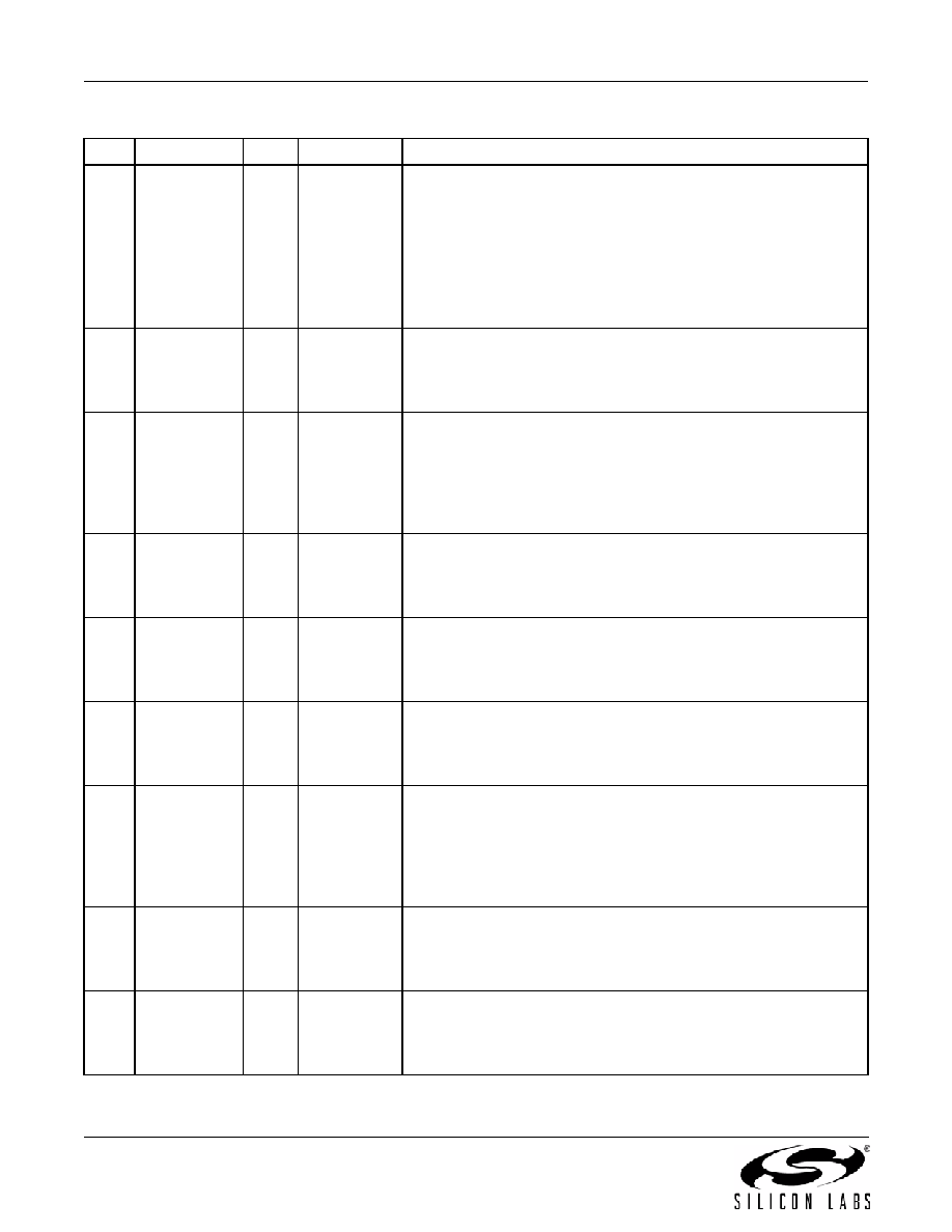
5,6
IN5/IN6
I
Multi
FDBK/FDBKB.
These pins can be used as a differential feedback input in zero
delay mode or as a secondary clock input. See section 3.2,
Figure 3, for termination details. See "3.10.6. Zero-Delay Mode" on
page 27 for zero delay mode set-up. Inputs to these pins must be
ac-coupled.
When not in use, leave IN5 unconnected and IN6 connected to
GND.
7
VDD
Supply
Core Supply Voltage.
This is the core supply voltage, which can operate from a 1.8, 2.5,
or 3.3 V supply. A 0.1 F bypass capacitor should be located very
close to this pin.
8
INTR
O
Open Drain
Interrupt.
A typical pullup resistor of 1–4 k
is used on this pin. This pin can
be pulled up to a supply voltage as high as 3.6 V regardless of the
other supply voltages on pins 7, 11, 15, 16, 20, and 24. The inter-
rupt condition allows the pull up resistor to pull the output up to the
supply voltage.
9
CLK3B
O
Multi
Output Clock B for Channel 3.
May be a single-ended output or half of a differential output with
CLK3A being the other differential half. If unused, leave this pin
floating.
10
CLK3A
O
Multi
Output Clock A for Channel 3.
May be a single-ended output or half of a differential output with
CLK3B being the other differential half. If unused, leave this pin
floating.
11
VDDO3
VDD
Supply
Output Clock Supply Voltage.
Supply voltage (3.3, 2.5, 1.8, or 1.5 V) for CLK3A,B. A 0.1 F
capacitor must be located very close to this pin. If CLK3 is not
used, this pin must be tied to VDD (pin 7, 24).
12
SCL
I
LVCMOS
I2C Serial Clock Input.
This is the serial clock input for the I2C bus. A pullup resistor at this
pin is required. Typical values would be 1–4 k
. See the I2C bus
spec for more information. This pin is 3.3 V tolerant regardless of
the other supply voltages on pins 7, 11, 15, 16, 20, 24. See Regis-
ter 27.
13
CLK2B
O
Multi
Output Clock B for Channel 2.
May be a single-ended output or half of a differential output with
CLK2A being the other differential half. If unused, leave this pin
floating.
14
CLK2A
O
Multi
Output Clock A for Channel 2.
May be a single-ended output or half of a differential output with
CLK2B being the other differential half. If unused, leave this pin
floating.
Table 16. Si5338 Pin Descriptions (Continued)
Pin #
Pin Name
I/O
Signal Type
Description
相关PDF资料 |
PDF描述 |
|---|---|
| AD5323BRUZ | IC DAC 12BIT DUAL R-R 16-TSSOP |
| SI5338M-A-GM | IC CLK GEN I2C BUS PROG 24QFN |
| AD5453YRMZ | IC DAC 14BIT MULTIPLYING 8-MSOP |
| ICS843156AKILFT | IC CLK GENERATOR 32VFQFP |
| VI-B0P-MY-F4 | CONVERTER MOD DC/DC 13.8V 50W |
相关代理商/技术参数 |
参数描述 |
|---|---|
| SI5338Q-A-GMR | 功能描述:时钟发生器及支持产品 I2C Program Clk Gen 0.16-200MHz 4Clk In RoHS:否 制造商:Silicon Labs 类型:Clock Generators 最大输入频率:14.318 MHz 最大输出频率:166 MHz 输出端数量:16 占空比 - 最大:55 % 工作电源电压:3.3 V 工作电源电流:1 mA 最大工作温度:+ 85 C 安装风格:SMD/SMT 封装 / 箱体:QFN-56 |
| Si5338Q-Axxxxx-GM | 制造商:Silicon Laboratories Inc 功能描述: |
| SI5338Q-B02153-GM | 制造商:Silicon Laboratories Inc 功能描述: 制造商:Silicon Laboratories Inc 功能描述:IC CLK GEN I2C BUS PROG 24QFN |
| Si5338Q-B-GM | 功能描述:时钟发生器及支持产品 I2C-prgrmmbl clock generatr .16-200 MHz RoHS:否 制造商:Silicon Labs 类型:Clock Generators 最大输入频率:14.318 MHz 最大输出频率:166 MHz 输出端数量:16 占空比 - 最大:55 % 工作电源电压:3.3 V 工作电源电流:1 mA 最大工作温度:+ 85 C 安装风格:SMD/SMT 封装 / 箱体:QFN-56 |
| Si5338Q-B-GMR | 功能描述:时钟发生器及支持产品 I2C Program Clk Gen 0.16-200MHz 4Clk In RoHS:否 制造商:Silicon Labs 类型:Clock Generators 最大输入频率:14.318 MHz 最大输出频率:166 MHz 输出端数量:16 占空比 - 最大:55 % 工作电源电压:3.3 V 工作电源电流:1 mA 最大工作温度:+ 85 C 安装风格:SMD/SMT 封装 / 箱体:QFN-56 |
发布紧急采购,3分钟左右您将得到回复。