- 您现在的位置:买卖IC网 > PDF目录98084 > SMQ320C32PCMM50 (TEXAS INSTRUMENTS INC) 24-BIT, 50 MHz, OTHER DSP, PQFP144 PDF资料下载
参数资料
| 型号: | SMQ320C32PCMM50 |
| 厂商: | TEXAS INSTRUMENTS INC |
| 元件分类: | 数字信号处理 |
| 英文描述: | 24-BIT, 50 MHz, OTHER DSP, PQFP144 |
| 封装: | PLASTIC, QFP-144 |
| 文件页数: | 48/50页 |
| 文件大小: | 674K |
| 代理商: | SMQ320C32PCMM50 |
第1页第2页第3页第4页第5页第6页第7页第8页第9页第10页第11页第12页第13页第14页第15页第16页第17页第18页第19页第20页第21页第22页第23页第24页第25页第26页第27页第28页第29页第30页第31页第32页第33页第34页第35页第36页第37页第38页第39页第40页第41页第42页第43页第44页第45页第46页第47页当前第48页第49页第50页
SMQ320C32
DIGITAL SIGNAL PROCESSOR
SGUS027B – APRIL 1998 – REVISED MARCH 1999
7
POST OFFICE BOX 1443
HOUSTON, TEXAS 77251–1443
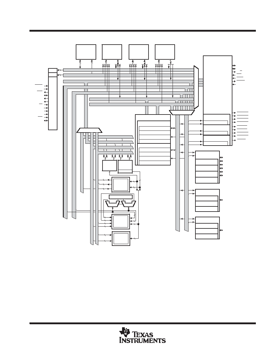
functional block diagram
Boot
ROM
Program
Cache
(64
× 32)
RAM
Block 0
(256
× 32)
RAM
Block 1
(256
× 32)
IR
PC
CPU1
REG1
REG2
Multiplexer
40
32
24
BK
ARAU0
ARAU1
DISP0, IR0, IR1
Extended-
Precision
Registers
(R0–R7)
Auxiliary
Registers
(AR0 – AR7)
Other
Registers
(12)
40
Multiplier
32-Bit
Barrel
Shifter
ALU
External
Memory
Interface
Serial Port
Data-Transmit
Register
Data-Receive
Register
FSX0
DX0
CLKX0
FSR0
DR0
CLKR0
Timer 0
Global-Control
Register
Timer-Period
Register
Timer-Counter
Register
TCLK0
Timer 1
Global-Control
Register
Timer-Period
Register
Timer-Counter
Register
TCLK1
PDATA Bus
PADDR Bus
DDATA Bus
DADDR1 Bus
DADDR2 Bus
DMADATA Bus
40
32
24
32
CPU2
32
40
Serial Port-
Control Reg.
Receive/Transmit
(R/X)Timer Register
Controller
Peripheral
Address
Bus
CPU1
REG1
REG2
DMAADDR Bus
STRB0 Control Reg.
STRB1 Control Reg.
IOSTRB Control Reg.
STRB1
IOSTRB
STRB0
Peripheral
Data
Bus
RESET
INT(3-0)
IACK
XF(1,0)
H1
H3
MCBL / MP
CLKIN
VDD
VSS
SHZ
EMU0–3
32
24
Multiplexer
A23 – A0
D31 – D0
R/W
RDY
HOLD
HOLDA
PRGW
STRB0_B3/A–1
STRB0_B2/A–2
STRB0_B1
STRB0_B0
IOSTRB
Multiplexer
DMA Controller
Global-Contol Register
Source-Address Register
Destination-Address Reg.
Transfer-Counter Reg.
DMA Channel 0
Global-Control Register
Source-Address Register
Destination-Address Reg.
Transfer-Counter Reg.
DMA Channel 1
STRB1_B3/A–1
STRB1_B2/A–2
STRB1_B1
STRB1_B0
operation
Operation of the SMQ320C32 is identical to the ’320C30 and ’320C31 digital signal processors, with the
exception of an enhanced external memory interface and the addition of two CPU power-management modes.
external memory interface
The SMQ320C32 has a configurable external memory interface with a 24-bit address bus, a 32-bit data bus,
and three independent multi-function strobes. The flexibility of this unique interface enables product designers
to minimize external memory-chip count.
相关PDF资料 |
PDF描述 |
|---|---|
| SN0305042RTHR | 1803 SERIES, LOW SKEW CLOCK DRIVER, 4 TRUE OUTPUT(S), 0 INVERTED OUTPUT(S), PQCC24 |
| SN2005118412ZHK | PCMCIA BUS CONTROLLER, PBGA216 |
| SNA7412ZHK | PCMCIA BUS CONTROLLER, PBGA216 |
| SN260Q | LOCAL AREA NETWORK CONTROLLER, QCC40 |
| SN54128J | TTL/H/L SERIES, QUAD 2-INPUT NOR GATE, CDIP14 |
相关代理商/技术参数 |
参数描述 |
|---|---|
| SMQ320C50 | 制造商:TI 制造商全称:Texas Instruments 功能描述:DIGITAL SIGNAL PROCESSOR |
| SMQ320C50GFA | 制造商:TI 制造商全称:Texas Instruments 功能描述:DIGITAL SIGNAL PROCESSOR |
| SMQ320C50HFG | 制造商:TI 制造商全称:Texas Instruments 功能描述:DIGITAL SIGNAL PROCESSOR |
| SMQ320C50PQ | 制造商:TI 制造商全称:Texas Instruments 功能描述:DIGITAL SIGNAL PROCESSOR |
| SMQ320C50PQM66 | 制造商:TI 制造商全称:Texas Instruments 功能描述:DIGITAL SIGNAL PROCESSOR |
发布紧急采购,3分钟左右您将得到回复。