参数资料
| 型号: | SN74ABT8952DW |
| 厂商: | Texas Instruments |
| 文件页数: | 5/31页 |
| 文件大小: | 0K |
| 描述: | IC SCAN-TEST-DEV/XCVR 28-SOIC |
| 标准包装: | 20 |
| 系列: | 74ABT |
| 逻辑类型: | 扫描测试设备,带寄存总线收发器 |
| 电源电压: | 4.5 V ~ 5.5 V |
| 位数: | 8 |
| 工作温度: | -40°C ~ 85°C |
| 安装类型: | 表面贴装 |
| 封装/外壳: | 28-SOIC(0.295",7.50mm 宽) |
| 供应商设备封装: | 28-SOIC |
| 包装: | 管件 |
| 产品目录页面: | 925 (CN2011-ZH PDF) |
| 其它名称: | 296-4116-5 |
第1页第2页第3页第4页当前第5页第6页第7页第8页第9页第10页第11页第12页第13页第14页第15页第16页第17页第18页第19页第20页第21页第22页第23页第24页第25页第26页第27页第28页第29页第30页第31页
SN54ABT8952, SN74ABT8952
SCAN TEST DEVICES WITH
OCTAL REGISTERED BUS TRANSCEIVERS
SCBS121D – AUGUST 1992 – REVISED JULY 1996
13
POST OFFICE BOX 655303
DALLAS, TEXAS 75265
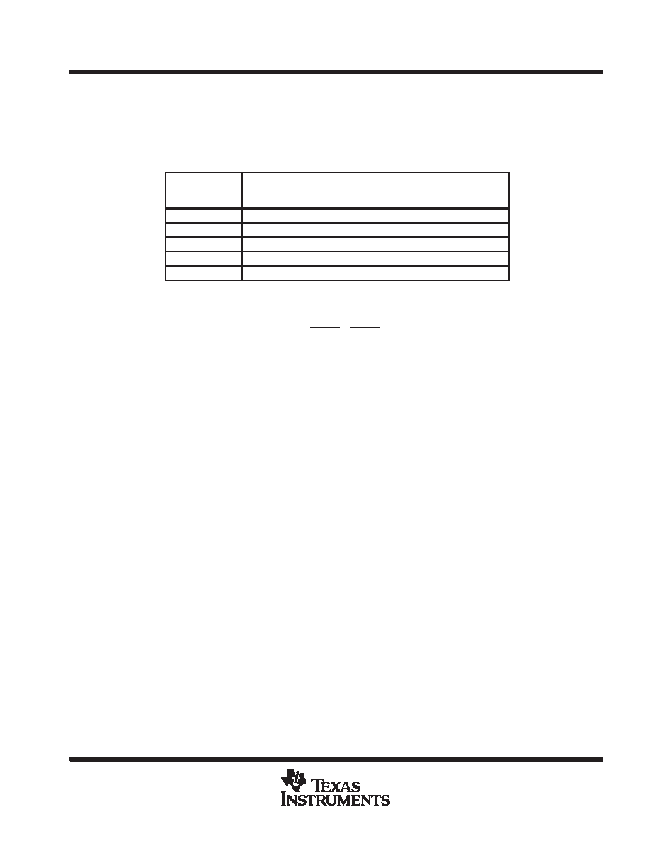
boundary-control register opcode description
The BCR opcodes are decoded from BCR bits 2–0 as shown in Table 4. The selected test operation is performed
while the RUNT instruction is executed in the Run-Test/Idle state. The following descriptions detail the operation
of each BCR instruction and illustrate the associated PSA and PRPG algorithms.
Table 4. Boundary-Control Register Opcodes
BINARY CODE
BIT 2
→ BIT 0
MSB
→ LSB
DESCRIPTION
X00
Sample inputs/toggle outputs (TOPSIP)
X01
Pseudo-random pattern generation/16-bit mode (PRPG)
X10
Parallel-signature analysis/16-bit mode (PSA)
011
Simultaneous PSA and PRPG/8-bit mode (PSA/PRPG)
111
Simultaneous PSA and binary count up/8-bit mode (PSA/COUNT)
In general, while the control input BSCs (bits 37–32) are not included in the sample, toggle, PSA, PRPG, or
COUNT algorithms, the output-enable BSCs (bits 37–36 of the BSR) do control the drive state (active or high
impedance) of the selected device output pins. These BCR instructions are valid only when the device is
operating in one direction of data flow (that is, OEAB
≠ OEBA). Otherwise, the bypass instruction is operated.
PSA input masking
Bits 10–3 of the BCR specify device input pins to be masked from PSA operations. Bit 10 selects masking for
device input pin A8 during A-to-B data flow or for device input pin B8 during B-to-A data flow. Bit 3 selects
masking for device input pins A1 or B1 during A-to-B or B-to-A data flow, respectively. Bits intermediate to 10
and 3 mask corresponding device input pins in order from most significant to least significant, as indicated in
Table 3. When the mask bit that corresponds to a particular device input has a logic 1 value, the device input
pin is masked from any PSA operation, i.e., that the state of the device input pin is ignored and has no effect
on the generated signature. Otherwise, when a mask bit has a logic 0 value, the corresponding device input
is not masked from the PSA operation.
sample inputs/toggle outputs (TOPSIP)
Data appearing at the selected device input pins is captured in the shift-register elements of the selected BSCs
on each rising edge of TCK. This data is updated in the shadow latches of the selected input BSCs and applied
to the inputs of the normal on-chip logic. Data in the shift-register elements of the selected output BSCs is
toggled on each rising edge of TCK, updated in the shadow latches, and applied to the associated device output
pins on each falling edge of TCK.
相关PDF资料 |
PDF描述 |
|---|---|
| V24B48M150BL3 | CONVERTER MOD DC/DC 48V 150W |
| MS27656E11A35SC | CONN RCPT 13POS WALL MNT W/SCKT |
| MS27468P17B99S | CONN RCPT 23POS JAM NUT W/SCKT |
| MS27513E18F35P | CONN RCPT 66POS BOX MNT W/PINS |
| MAX3227ECUE+T | IC TXRX RS232 1MBPS SD 16TSSOP |
相关代理商/技术参数 |
参数描述 |
|---|---|
| SN74ABT8952DWE4 | 功能描述:特定功能逻辑 Device w/Octal Rgstr Bus Transceiver RoHS:否 制造商:Texas Instruments 产品: 系列:SN74ABTH18502A 工作电源电压:5 V 封装 / 箱体:LQFP-64 封装:Tube |
| SN74ABT8952DWG4 | 功能描述:特定功能逻辑 Scan Test Devices RoHS:否 制造商:Texas Instruments 产品: 系列:SN74ABTH18502A 工作电源电压:5 V 封装 / 箱体:LQFP-64 封装:Tube |
| SN74ABT8952DWR | 功能描述:特定功能逻辑 Device w/Octal Rgstr Bus Transceiver RoHS:否 制造商:Texas Instruments 产品: 系列:SN74ABTH18502A 工作电源电压:5 V 封装 / 箱体:LQFP-64 封装:Tube |
| SN74ABT8952DWRE4 | 功能描述:特定功能逻辑 Device w/Octal Rgstr Bus Transceiver RoHS:否 制造商:Texas Instruments 产品: 系列:SN74ABTH18502A 工作电源电压:5 V 封装 / 箱体:LQFP-64 封装:Tube |
| SN74ABT8952DWRG4 | 功能描述:特定功能逻辑 Scan Test Devices RoHS:否 制造商:Texas Instruments 产品: 系列:SN74ABTH18502A 工作电源电压:5 V 封装 / 箱体:LQFP-64 封装:Tube |
发布紧急采购,3分钟左右您将得到回复。