- 您现在的位置:买卖IC网 > PDF目录98141 > SPAK56855BU120 (FREESCALE SEMICONDUCTOR INC) 16-BIT, 4 MHz, OTHER DSP, PQFP100 PDF资料下载
参数资料
| 型号: | SPAK56855BU120 |
| 厂商: | FREESCALE SEMICONDUCTOR INC |
| 元件分类: | 数字信号处理 |
| 英文描述: | 16-BIT, 4 MHz, OTHER DSP, PQFP100 |
| 封装: | LQFP-100 |
| 文件页数: | 627/649页 |
| 文件大小: | 7965K |
| 代理商: | SPAK56855BU120 |
第1页第2页第3页第4页第5页第6页第7页第8页第9页第10页第11页第12页第13页第14页第15页第16页第17页第18页第19页第20页第21页第22页第23页第24页第25页第26页第27页第28页第29页第30页第31页第32页第33页第34页第35页第36页第37页第38页第39页第40页第41页第42页第43页第44页第45页第46页第47页第48页第49页第50页第51页第52页第53页第54页第55页第56页第57页第58页第59页第60页第61页第62页第63页第64页第65页第66页第67页第68页第69页第70页第71页第72页第73页第74页第75页第76页第77页第78页第79页第80页第81页第82页第83页第84页第85页第86页第87页第88页第89页第90页第91页第92页第93页第94页第95页第96页第97页第98页第99页第100页第101页第102页第103页第104页第105页第106页第107页第108页第109页第110页第111页第112页第113页第114页第115页第116页第117页第118页第119页第120页第121页第122页第123页第124页第125页第126页第127页第128页第129页第130页第131页第132页第133页第134页第135页第136页第137页第138页第139页第140页第141页第142页第143页第144页第145页第146页第147页第148页第149页第150页第151页第152页第153页第154页第155页第156页第157页第158页第159页第160页第161页第162页第163页第164页第165页第166页第167页第168页第169页第170页第171页第172页第173页第174页第175页第176页第177页第178页第179页第180页第181页第182页第183页第184页第185页第186页第187页第188页第189页第190页第191页第192页第193页第194页第195页第196页第197页第198页第199页第200页第201页第202页第203页第204页第205页第206页第207页第208页第209页第210页第211页第212页第213页第214页第215页第216页第217页第218页第219页第220页第221页第222页第223页第224页第225页第226页第227页第228页第229页第230页第231页第232页第233页第234页第235页第236页第237页第238页第239页第240页第241页第242页第243页第244页第245页第246页第247页第248页第249页第250页第251页第252页第253页第254页第255页第256页第257页第258页第259页第260页第261页第262页第263页第264页第265页第266页第267页第268页第269页第270页第271页第272页第273页第274页第275页第276页第277页第278页第279页第280页第281页第282页第283页第284页第285页第286页第287页第288页第289页第290页第291页第292页第293页第294页第295页第296页第297页第298页第299页第300页第301页第302页第303页第304页第305页第306页第307页第308页第309页第310页第311页第312页第313页第314页第315页第316页第317页第318页第319页第320页第321页第322页第323页第324页第325页第326页第327页第328页第329页第330页第331页第332页第333页第334页第335页第336页第337页第338页第339页第340页第341页第342页第343页第344页第345页第346页第347页第348页第349页第350页第351页第352页第353页第354页第355页第356页第357页第358页第359页第360页第361页第362页第363页第364页第365页第366页第367页第368页第369页第370页第371页第372页第373页第374页第375页第376页第377页第378页第379页第380页第381页第382页第383页第384页第385页第386页第387页第388页第389页第390页第391页第392页第393页第394页第395页第396页第397页第398页第399页第400页第401页第402页第403页第404页第405页第406页第407页第408页第409页第410页第411页第412页第413页第414页第415页第416页第417页第418页第419页第420页第421页第422页第423页第424页第425页第426页第427页第428页第429页第430页第431页第432页第433页第434页第435页第436页第437页第438页第439页第440页第441页第442页第443页第444页第445页第446页第447页第448页第449页第450页第451页第452页第453页第454页第455页第456页第457页第458页第459页第460页第461页第462页第463页第464页第465页第466页第467页第468页第469页第470页第471页第472页第473页第474页第475页第476页第477页第478页第479页第480页第481页第482页第483页第484页第485页第486页第487页第488页第489页第490页第491页第492页第493页第494页第495页第496页第497页第498页第499页第500页第501页第502页第503页第504页第505页第506页第507页第508页第509页第510页第511页第512页第513页第514页第515页第516页第517页第518页第519页第520页第521页第522页第523页第524页第525页第526页第527页第528页第529页第530页第531页第532页第533页第534页第535页第536页第537页第538页第539页第540页第541页第542页第543页第544页第545页第546页第547页第548页第549页第550页第551页第552页第553页第554页第555页第556页第557页第558页第559页第560页第561页第562页第563页第564页第565页第566页第567页第568页第569页第570页第571页第572页第573页第574页第575页第576页第577页第578页第579页第580页第581页第582页第583页第584页第585页第586页第587页第588页第589页第590页第591页第592页第593页第594页第595页第596页第597页第598页第599页第600页第601页第602页第603页第604页第605页第606页第607页第608页第609页第610页第611页第612页第613页第614页第615页第616页第617页第618页第619页第620页第621页第622页第623页第624页第625页第626页当前第627页第628页第629页第630页第631页第632页第633页第634页第635页第636页第637页第638页第639页第640页第641页第642页第643页第644页第645页第646页第647页第648页第649页
Power, Ground and Peripheral Signals
MOTOROLA
Pin Descriptions
2-11
Preliminary
2
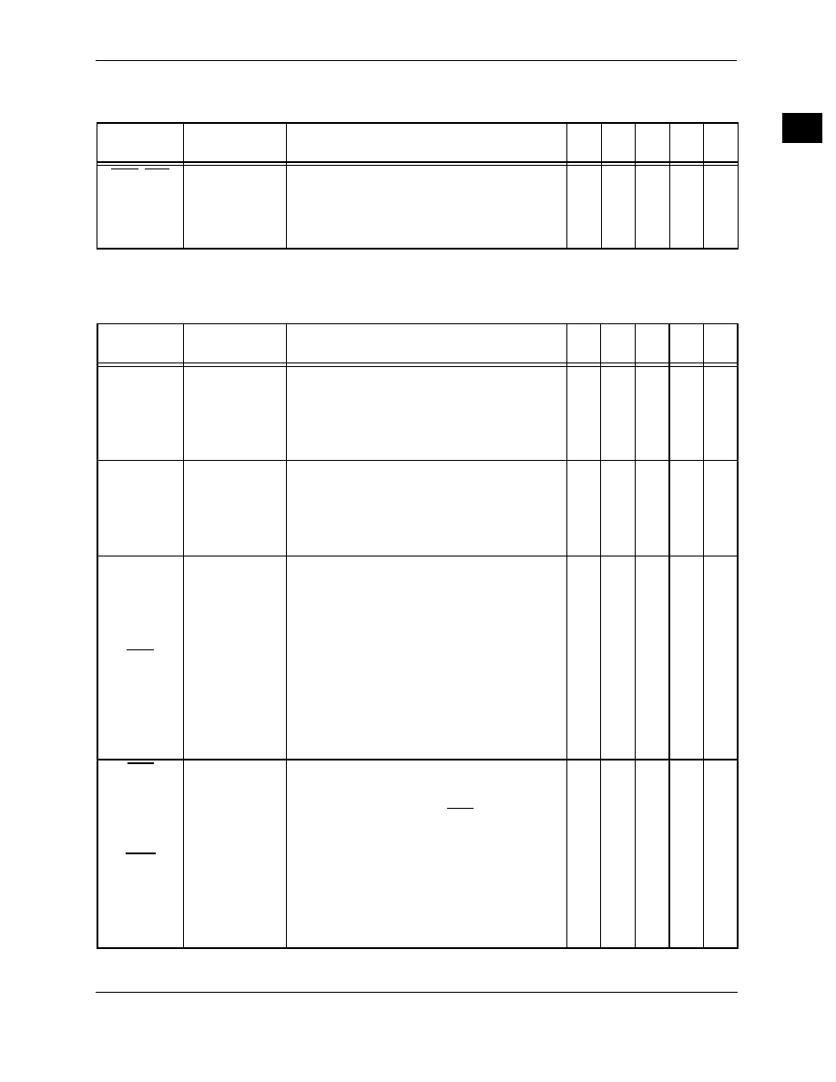
Table 2-5.
External Chip Select
Signal Name
Signal Type
853
Pins
854
Pins
855
Pins
857
Pins
858
Pins
CSO- CS3
(GPIOA0-A3)
Output
Input / Output
External Chip Select—These pins are used as
chip selects during external memory cycles.
Port A GPIO0-3—These are General Purpose I/O
pins when not configured for EMI use.
44
4
Table 2-6. Host Interface Eight
Signal Name
Signal Type
853
Pins
854
Pins
855
Pins
857
Pins
858
Pins
HD0-HD7
(GPIOB0-B7)
Input
Input / Output
Host Data—These inputs provide data for the HI
registers. These pins are disconnected internally
during reset.
Port B GPIO 0-7—These are a General Purpose
I/O pins when not configured for host port use.
88
—
88
HA0-HA2
(GPIOB8-B10)
Input
Input / Output
Host Address—These inputs provide address
selection for HI registers. These pins are
disconnected internally during reset.
Port B GPIO 10—These are General Purpose I/O
pins when not configured for host port use.
33
—
33
HRWB
(HRD)
(GPIOB11)
Input
Input
Input / Output
Host Read/Write—When the HI is programmed to
interface to a single-data-strobe host bus and the
HI function is selected, this signal is the
Read/Write input. These pins are disconnected
internally during reset.
Host Read Enable—This signal is the Read Data
input when the HI is programmed to interface to a
double-data-strobe host bus and the HI function is
selected.
Port B GPIO 11—This is a General Purpose I/O
pin when not configured for host port use.
11
—
11
HDS
(HRW)
(GPIOB12)
Input
Input
Input / Output
Host Data Strobe—When the HI is programmed
to interface to a single-data-strobe host bus and
the HI function is selected, this input enables a
data transfer on the HI when HCS is asserted.
Host Write Enable—This signal is the Write Data
input when the HI is programmed to interface to a
double-data-strobe host bus and the HI function is
selected.
Port B GPIO 12—This is a General Purpose I/O
pin when not configured for host port use.
11
—
11
相关PDF资料 |
PDF描述 |
|---|---|
| SPAK56854FG120 | 16-BIT, 4 MHz, OTHER DSP, PQFP128 |
| SPAK56F802TA60 | 0-BIT, 60 MHz, OTHER DSP, PQFP32 |
| SPAK56F805FV80 | 16-BIT, 8 MHz, OTHER DSP, PQFP144 |
| SPAK56F807VF80 | 16-BIT, 80 MHz, OTHER DSP, PBGA160 |
| SPAK56F807VF80 | 16-BIT, 80 MHz, OTHER DSP, PBGA160 |
相关代理商/技术参数 |
参数描述 |
|---|---|
| SPAK56857BU120 | 制造商:MOTOROLA 制造商全称:Motorola, Inc 功能描述:120 MIPS Hybrid Processor |
| SPAK56F803BU80 | 制造商:Freescale Semiconductor 功能描述: |
| SPAK56F805FV80 | 制造商:Freescale Semiconductor 功能描述: |
| SPAKDSP303AG100 | 功能描述:数字信号处理器和控制器 - DSP, DSC SPAKDSP303AG100 RoHS:否 制造商:Microchip Technology 核心:dsPIC 数据总线宽度:16 bit 程序存储器大小:16 KB 数据 RAM 大小:2 KB 最大时钟频率:40 MHz 可编程输入/输出端数量:35 定时器数量:3 设备每秒兆指令数:50 MIPs 工作电源电压:3.3 V 最大工作温度:+ 85 C 封装 / 箱体:TQFP-44 安装风格:SMD/SMT |
| SPAKDSP303GC100 | 制造商:Motorola Inc 功能描述: |
发布紧急采购,3分钟左右您将得到回复。