- 您现在的位置:买卖IC网 > PDF目录297473 > SST32HF1621C-90-4C-LS (SILICON STORAGE TECHNOLOGY INC) SPECIALTY MEMORY CIRCUIT, PBGA62 PDF资料下载
参数资料
| 型号: | SST32HF1621C-90-4C-LS |
| 厂商: | SILICON STORAGE TECHNOLOGY INC |
| 元件分类: | 存储器 |
| 英文描述: | SPECIALTY MEMORY CIRCUIT, PBGA62 |
| 封装: | 8 X 10 MM, 1.40 MM HEIGHT, MO-210, LFBGA-62 |
| 文件页数: | 32/37页 |
| 文件大小: | 451K |
| 代理商: | SST32HF1621C-90-4C-LS |
第1页第2页第3页第4页第5页第6页第7页第8页第9页第10页第11页第12页第13页第14页第15页第16页第17页第18页第19页第20页第21页第22页第23页第24页第25页第26页第27页第28页第29页第30页第31页当前第32页第33页第34页第35页第36页第37页
4
Preliminary Specifications
Multi-Purpose Flash Plus + SRAM ComboMemory
SST32HF1641 / SST32HF1681 / SST32HF3241 / SST32HF3281 / SST32HF6481
SST32HF1621C / SST32HF1641C / SST32HF3241C
2004 Silicon Storage Technology, Inc.
S71236-02-000
6/04
The actual completion of the nonvolatile write is asynchro-
nous with the system; therefore, either a Data# Polling or
Toggle Bit read may be simultaneous with the completion
of the Write cycle. If this occurs, the system may possibly
get an erroneous result, i.e., valid data may appear to con-
flict with either DQ7 or DQ6. In order to prevent spurious
rejection, if an erroneous result occurs, the software routine
should include a loop to read the accessed location an
additional two (2) times. If both reads are valid, then the
device has completed the Write cycle, otherwise the rejec-
tion is valid.
Flash Data# Polling (DQ7)
When the SST32HFx1/x1C flash memory banks are in the
internal Program operation, any attempt to read DQ7 will
produce the complement of the true data. Once the Pro-
gram operation is completed, DQ7 will produce true data.
Note that even though DQ7 may have valid data immedi-
ately following the completion of an internal Write opera-
tion, the remaining data outputs may still be invalid: valid
data on the entire data bus will appear in subsequent suc-
cessive Read cycles after an interval of 1 s. During inter-
nal Erase operation, any attempt to read DQ7 will produce
a ‘0’. Once the internal Erase operation is completed, DQ7
will produce a ‘1’. The Data# Polling is valid after the rising
edge of the fourth WE# (or BEF#) pulse for Program opera-
tion. For Sector- or Block-Erase, the Data# Polling is valid
after the rising edge of the sixth WE# (or BEF#) pulse. See
for a flowchart.
Toggle Bits (DQ6 and DQ2)
During the internal Program or Erase operation, any con-
secutive attempts to read DQ6 will produce alternating “1”s
and “0”s, i.e., toggling between 1 and 0. When the internal
Program or Erase operation is completed, the DQ6 bit will
stop toggling. The device is then ready for the next opera-
tion. For Sector-, Block-, or Chip-Erase, the toggle bit (DQ6)
is valid after the rising edge of sixth WE# (or BEF#) pulse.
DQ6 will be set to “1” if a Read operation is attempted on an
Erase-Suspended Sector/Block. If Program operation is ini-
tiated in a sector/block not selected in Erase-Suspend
mode, DQ6 will toggle.
An additional Toggle Bit is available on DQ2, which can be
used in conjunction with DQ6 to check whether a particular
sector is being actively erased or erase-suspended. Table 1
shows detailed status bits information. The Toggle Bit
(DQ2) is valid after the rising edge of the last WE# (or
BEF#) pulse of Write operation. See Figure 11 for Toggle
Bit timing diagram and Figure 23 for a flowchart.
Note: DQ7 and DQ2 require a valid address when reading
status information.
Flash Memory Data Protection
The SST32HFx1/x1C flash memory bank provides both
hardware and software features to protect nonvolatile data
from inadvertent writes.
Flash Hardware Data Protection
Noise/Glitch Protection: A WE# or BEF# pulse of less than
5 ns will not initiate a Write cycle.
VDD Power Up/Down Detection: The Write operation is
inhibited when VDD is less than 1.5V.
Write Inhibit Mode: Forcing OE# low, BEF# high, or WE#
high will inhibit the flash Write operation. This prevents
inadvertent writes during power-up or power-down.
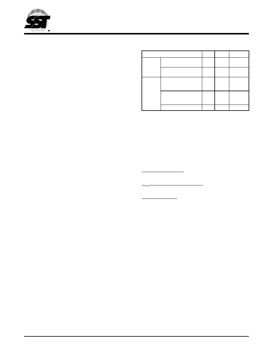
TABLE
1: WRITE OPERATION STATUS
Status
DQ7
DQ6
DQ2
Normal
Operation
Standard
Program
DQ7#
Toggle
No Toggle
Standard
Erase
0
Toggle
Erase-
Suspend
Mode
Read from
Erase-Suspended
Sector/Block
1
Toggle
Read from
Non- Erase-Suspended
Sector/Block
Data
Program
DQ7#
Toggle
N/A
T1.0 1236
相关PDF资料 |
PDF描述 |
|---|---|
| SST34HF1602C-70-4C-B1P | SPECIALTY MEMORY CIRCUIT, PBGA56 |
| SST42AAA | LATCHING INTERVAL-DELAY RELAY, DPDT, LATCHED, 120VDC (COIL), 3000mW (COIL), 0.1-10s, SOCKET MOUNT |
| SST42ADA | LATCHING INTERVAL-DELAY RELAY, DPDT, LATCHED, 120VDC (COIL), 3000mW (COIL), 1.8-180s, SOCKET MOUNT |
| SST42AEA | LATCHING INTERVAL-DELAY RELAY, DPDT, LATCHED, 120VDC (COIL), 3000mW (COIL), 3-300s, SOCKET MOUNT |
| SST42AGA | LATCHING INTERVAL-DELAY RELAY, DPDT, LATCHED, 120VDC (COIL), 3000mW (COIL), 18-1800s, SOCKET MOUNT |
相关代理商/技术参数 |
参数描述 |
|---|---|
| SST32HF1622C | 制造商:SST 制造商全称:Silicon Storage Technology, Inc 功能描述:Multi-Purpose Flash Plus + SRAM ComboMemory |
| SST32HF1622C-70-4C-LFS | 制造商:SST 制造商全称:Silicon Storage Technology, Inc 功能描述:Multi-Purpose Flash Plus + SRAM ComboMemory |
| SST32HF1622C-70-4C-LFSE | 制造商:SST 制造商全称:Silicon Storage Technology, Inc 功能描述:Multi-Purpose Flash Plus + SRAM ComboMemory |
| SST32HF1622C-70-4C-LS | 制造商:SST 制造商全称:Silicon Storage Technology, Inc 功能描述:Multi-Purpose Flash Plus + SRAM ComboMemory |
| SST32HF1622C-70-4C-LSE | 制造商:SST 制造商全称:Silicon Storage Technology, Inc 功能描述:Multi-Purpose Flash Plus + SRAM ComboMemory |
发布紧急采购,3分钟左右您将得到回复。