- 您现在的位置:买卖IC网 > PDF目录98143 > SSTUAF32869AHLFT (INTEGRATED DEVICE TECHNOLOGY INC) 32869 SERIES, POSITIVE EDGE TRIGGERED D FLIP-FLOP, TRUE OUTPUT, PBGA150 PDF资料下载
参数资料
| 型号: | SSTUAF32869AHLFT |
| 厂商: | INTEGRATED DEVICE TECHNOLOGY INC |
| 元件分类: | 锁存器 |
| 英文描述: | 32869 SERIES, POSITIVE EDGE TRIGGERED D FLIP-FLOP, TRUE OUTPUT, PBGA150 |
| 封装: | LEAD FREE, BGA-150 |
| 文件页数: | 20/20页 |
| 文件大小: | 452K |
| 代理商: | SSTUAF32869AHLFT |
ICSSSTUAF32869A
14-BIT CONFIGURABLE REGISTERED BUFFER FOR DDR2
COMMERCIAL TEMPERATURE GRADE
14-BIT CONFIGURABLE REGISTERED BUFFER FOR DDR2
9
ICSSSTUAF32869A
7095/14
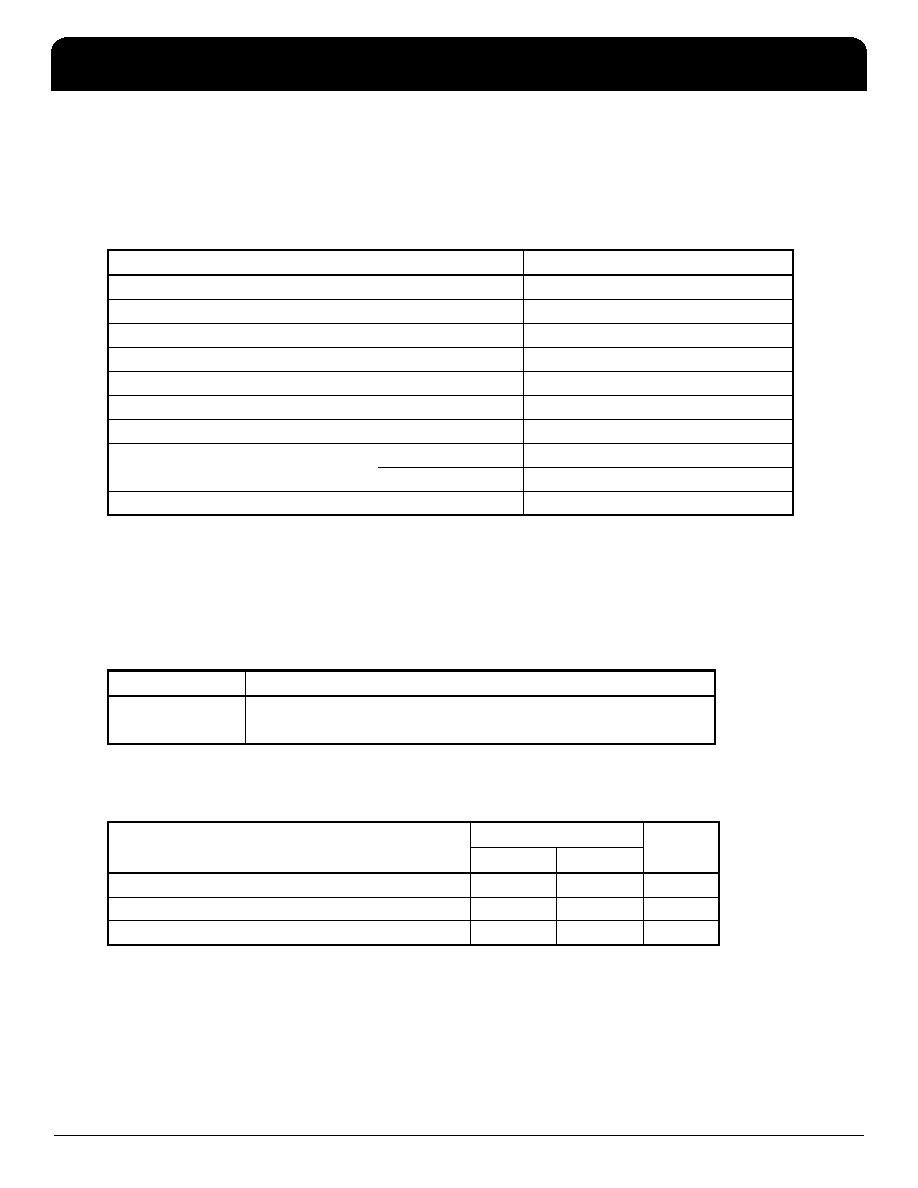
Absolute Maximum Ratings
Stresses greater than those listed under ABSOLUTE MAXIMUM RATINGS may cause permanent damage to the
device. This is a stress rating only and functional operation of the device at these or any other conditions above
those indicated in the operational sections of this specification is not implied. Exposure to absolute maximum rating
conditions for extended periods may affect reliability.
Mode Select
Output Buffer Characteristics
Output edge rates over recommended operating free-air temperature range
Item
Rating
Supply Voltage, VDD
-0.5V to 2.5V
Input Voltage Range, VI1
1
The input and output negative voltage ratings may be exceeded if the ratings of the I/P and
O/P clamp current are observed.
-0.5V to VDD + 2.5V
Output Voltage Range, VO1,2
2
This current will flow only when the output is in the high state level VO > VDDQ.
-0.5V to VDDQ + 0.5V
Input Clamp Current, IIK
±50mA
Output Clamp Current, IOK
±50mA
Continuous Output Clamp Current, IO
±50mA
Continuous Current through each VDD or GND
±100mA
Package Thermal Impedance (
θja)3
3
The package thermal impedance is calculated in accordance with JESD 51.
0m/s Airflow
40
° C/W
1m/s Airflow
29
° C/W
Storage Temperature
-65 to +150
° C
C1
Device Mode
0
First device in pair, Front
1
Second device in pair, Back
Parameter
VDD = 1.8V ± 0.1V
Units
Min.
Max.
dV/dt_r
1
4
V/ns
dV/dt_f
1
4
V/ns
dV/dt_
1
1
Difference between dV/dt_r (rising edge rate) and dV/dt_f (falling edge rate).
1V/ns
相关PDF资料 |
PDF描述 |
|---|---|
| SSTUB32864EC/G | 32864 SERIES, POSITIVE EDGE TRIGGERED D FLIP-FLOP, COMPLEMENTARY OUTPUT, PBGA96 |
| SSTUB32868ET/S | 32868 SERIES, POSITIVE EDGE TRIGGERED D FLIP-FLOP, TRUE OUTPUT, PBGA176 |
| SSTUG32865ET/S | SSTU SERIES, POSITIVE EDGE TRIGGERED D FLIP-FLOP, TRUE OUTPUT, PBGA160 |
| SSTUG32868ET/G | 32868 SERIES, POSITIVE EDGE TRIGGERED D FLIP-FLOP, COMPLEMENTARY OUTPUT, PBGA176 |
| SSTUP32866EC/S | 32866 SERIES, POSITIVE EDGE TRIGGERED D FLIP-FLOP, COMPLEMENTARY OUTPUT, PBGA96 |
相关代理商/技术参数 |
参数描述 |
|---|---|
| SSTUB32864 | 制造商:PHILIPS 制造商全称:NXP Semiconductors 功能描述:1.8 V configurable registered buffer for DDR2-800 RDIMM applications |
| SSTUB32864AHLF | 功能描述:IC REGIST BUFF 25BIT DDR2 96-BGA RoHS:是 类别:集成电路 (IC) >> 逻辑 - 专用逻辑 系列:- 产品变化通告:Product Discontinuation 25/Apr/2012 标准包装:1,500 系列:74SSTV 逻辑类型:DDR 的寄存缓冲器 电源电压:2.3 V ~ 2.7 V 位数:14 工作温度:0°C ~ 70°C 安装类型:表面贴装 封装/外壳:48-TFSOP(0.240",6.10mm 宽) 供应商设备封装:48-TSSOP 包装:带卷 (TR) |
| SSTUB32864AHLFT | 功能描述:IC REGIST BUFF 25BIT DDR2 96-BGA RoHS:是 类别:集成电路 (IC) >> 逻辑 - 专用逻辑 系列:- 产品变化通告:Product Discontinuation 25/Apr/2012 标准包装:1,500 系列:74SSTV 逻辑类型:DDR 的寄存缓冲器 电源电压:2.3 V ~ 2.7 V 位数:14 工作温度:0°C ~ 70°C 安装类型:表面贴装 封装/外壳:48-TFSOP(0.240",6.10mm 宽) 供应商设备封装:48-TSSOP 包装:带卷 (TR) |
| SSTUB32864BHLF | 功能描述:寄存器 RoHS:否 制造商:NXP Semiconductors 逻辑类型:CMOS 逻辑系列:HC 电路数量:1 最大时钟频率:36 MHz 传播延迟时间: 高电平输出电流:- 7.8 mA 低电平输出电流:7.8 mA 电源电压-最大:6 V 最大工作温度:+ 125 C 封装 / 箱体:SOT-38 封装:Tube |
| SSTUB32864BHLFT | 功能描述:寄存器 RoHS:否 制造商:NXP Semiconductors 逻辑类型:CMOS 逻辑系列:HC 电路数量:1 最大时钟频率:36 MHz 传播延迟时间: 高电平输出电流:- 7.8 mA 低电平输出电流:7.8 mA 电源电压-最大:6 V 最大工作温度:+ 125 C 封装 / 箱体:SOT-38 封装:Tube |
发布紧急采购,3分钟左右您将得到回复。