- 您现在的位置:买卖IC网 > PDF目录271212 > ST10F273M-4QR3 (STMICROELECTRONICS) 16-BIT, FLASH, 64 MHz, MICROCONTROLLER, PQFP144 PDF资料下载
参数资料
| 型号: | ST10F273M-4QR3 |
| 厂商: | STMICROELECTRONICS |
| 元件分类: | 微控制器/微处理器 |
| 英文描述: | 16-BIT, FLASH, 64 MHz, MICROCONTROLLER, PQFP144 |
| 封装: | 28 X 28 MM, 3.40 MM HEIGHT, 0.65 MM PITCH, PLASTIC, QFP-144 |
| 文件页数: | 44/182页 |
| 文件大小: | 3222K |
| 代理商: | ST10F273M-4QR3 |
第1页第2页第3页第4页第5页第6页第7页第8页第9页第10页第11页第12页第13页第14页第15页第16页第17页第18页第19页第20页第21页第22页第23页第24页第25页第26页第27页第28页第29页第30页第31页第32页第33页第34页第35页第36页第37页第38页第39页第40页第41页第42页第43页当前第44页第45页第46页第47页第48页第49页第50页第51页第52页第53页第54页第55页第56页第57页第58页第59页第60页第61页第62页第63页第64页第65页第66页第67页第68页第69页第70页第71页第72页第73页第74页第75页第76页第77页第78页第79页第80页第81页第82页第83页第84页第85页第86页第87页第88页第89页第90页第91页第92页第93页第94页第95页第96页第97页第98页第99页第100页第101页第102页第103页第104页第105页第106页第107页第108页第109页第110页第111页第112页第113页第114页第115页第116页第117页第118页第119页第120页第121页第122页第123页第124页第125页第126页第127页第128页第129页第130页第131页第132页第133页第134页第135页第136页第137页第138页第139页第140页第141页第142页第143页第144页第145页第146页第147页第148页第149页第150页第151页第152页第153页第154页第155页第156页第157页第158页第159页第160页第161页第162页第163页第164页第165页第166页第167页第168页第169页第170页第171页第172页第173页第174页第175页第176页第177页第178页第179页第180页第181页第182页
Electrical characteristics
ST10F273M
138/182
24.7.1
Conversion timing control
When a conversion is started, first the capacitances of the converter are loaded via the
respective analog input pin to the current analog input voltage. The time to load the
capacitances is referred to as sample time. Next the sampled voltage is converted to a
digital value several successive steps, which correspond to the 10-bit resolution of the ADC.
During these steps the internal capacitances are repeatedly charged and discharged via the
VAREF pin.
The current that has to be drawn from the sources for sampling and changing charges
depends on the time that each respective step takes, because the capacitors must reach
their final voltage level within the given time, at least with a certain approximation. The
maximum current, however, that a source can deliver, depends on its internal resistance.
The time that the two different actions (sampling, and converting) take during conversion
can be programmed within a certain range in the ST10F273M relative to the CPU clock. The
absolute time that is consumed by the different conversion steps therefore is independent
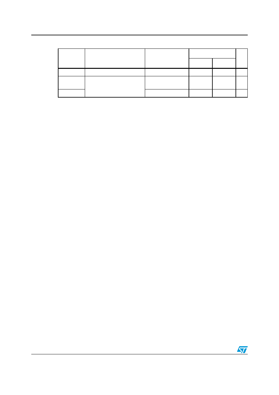
CS
CC
Sampling capacitance(3)(8)
–3.5
pF
RSW
CC
Analog switch resistance(3)(8)
Port5
Port1
–
600
1600
RAD
CC
–
1300
1.
VAREF can be tied to ground when A/D converter is not in use: An extra consumption (around 200A) on
main VDD is added due to internal analog circuitry not completely turned off. Therefore, it is suggested to
maintain the VAREF at VDD level even when not in use, and eventually switch off the A/D converter circuitry
by setting bit ADOFF in ADCON register.
2.
VAIN may exceed VAGND or VAREF up to the absolute maximum ratings. However, the conversion result in
these cases will be 0x000H or 0x3FFH, respectively.
3.
Not 100% tested, guaranteed by design characterization.
4.
During the sample time the input capacitance CAIN can be charged/discharged by the external source. The
internal resistance of the analog source must allow the capacitance to reach its final voltage level within tS.
After the end of the sample time tS, changes of the analog input voltage have no effect on the conversion
result.
5.
This parameter includes the sample time tS, the time for determining the digital result and the time to load
the result register with the conversion result. Values for the conversion clock tCC depend on programming
and can be taken from next Table 61.
6.
DNL, INL, OFS and TUE are tested at VAREF = 5.0 V, VAGND = 0V, VDD = 5.0 V. It is guaranteed by design
characterization for all other voltages within the defined voltage range.
‘LSB’ has a value of VAREF/1024.
For Port5 channels, the specified TUE (± 2LSB) is guaranteed also with an overload condition (see IOV
specification) occurring on maximum 2 not selected analog input pins of Port5 and if the absolute sum of
input overload currents on all Port5 analog input pins does not exceed 10 mA.
For Port1 channels, the specified TUE is guaranteed when no overload condition is applied to Port1 pins:
When an overload condition occurs on maximum 2 not selected analog input pins of Port1 and the input
positive overload current on all analog input pins does not exceed 10 mA (either dynamic or static
injection), the specified TUE is degraded (± 7LSB). To acheive the same accuracy, the negative injection
current on Port1 pins must not exceed -1mA in case of both dynamic and static injection.
7.
The coupling factor is measured on a channel while an overload condition occurs on the adjacent not
selected channels with the overload current within the different specified ranges (for both positive and
negative injection current).
8.
Refer to scheme in Figure 41.
Table 60.
A/D converter characteristics (continued)
Symbol
Parameter
Test condition
Limit values
Unit
Min
Max
相关PDF资料 |
PDF描述 |
|---|---|
| ST72P325J6TB/XXXRE | 8-BIT, MROM, 8 MHz, MICROCONTROLLER, PQFP44 |
| ST72P325J9TB/XXXRE | 8-BIT, MROM, 8 MHz, MICROCONTROLLER, PQFP44 |
| ST72314J4TC/XXX | 8-BIT, MROM, 8 MHz, MICROCONTROLLER, PQFP44 |
| S9S08SH4E2MTJR | 8-BIT, FLASH, 16 MHz, MICROCONTROLLER, PDSO20 |
| S9S08SH8E2MTG | 8-BIT, FLASH, 16 MHz, MICROCONTROLLER, PDSO16 |
相关代理商/技术参数 |
参数描述 |
|---|---|
| ST10F273M-4T3 | 功能描述:16位微控制器 - MCU 16-bit MCU 512 Kbyte Flash memory 36 Kbyt RoHS:否 制造商:Texas Instruments 核心:RISC 处理器系列:MSP430FR572x 数据总线宽度:16 bit 最大时钟频率:24 MHz 程序存储器大小:8 KB 数据 RAM 大小:1 KB 片上 ADC:Yes 工作电源电压:2 V to 3.6 V 工作温度范围:- 40 C to + 85 C 封装 / 箱体:VQFN-40 安装风格:SMD/SMT |
| ST10F273M-4TR3 | 功能描述:16位微控制器 - MCU 16-bit MCU 512 Kbyte Flash memory 36 Kbyt RoHS:否 制造商:Texas Instruments 核心:RISC 处理器系列:MSP430FR572x 数据总线宽度:16 bit 最大时钟频率:24 MHz 程序存储器大小:8 KB 数据 RAM 大小:1 KB 片上 ADC:Yes 工作电源电压:2 V to 3.6 V 工作温度范围:- 40 C to + 85 C 封装 / 箱体:VQFN-40 安装风格:SMD/SMT |
| ST10F273Z4Q3 | 功能描述:16位微控制器 - MCU 16B MCU RoHS:否 制造商:Texas Instruments 核心:RISC 处理器系列:MSP430FR572x 数据总线宽度:16 bit 最大时钟频率:24 MHz 程序存储器大小:8 KB 数据 RAM 大小:1 KB 片上 ADC:Yes 工作电源电压:2 V to 3.6 V 工作温度范围:- 40 C to + 85 C 封装 / 箱体:VQFN-40 安装风格:SMD/SMT |
| ST10F273Z4T3 | 功能描述:16位微控制器 - MCU 16B MCU RoHS:否 制造商:Texas Instruments 核心:RISC 处理器系列:MSP430FR572x 数据总线宽度:16 bit 最大时钟频率:24 MHz 程序存储器大小:8 KB 数据 RAM 大小:1 KB 片上 ADC:Yes 工作电源电压:2 V to 3.6 V 工作温度范围:- 40 C to + 85 C 封装 / 箱体:VQFN-40 安装风格:SMD/SMT |
| ST10F274Z2T7 | 制造商:STMicroelectronics 功能描述:832K FLASH PQFP 144 - Trays |
发布紧急采购,3分钟左右您将得到回复。