- 您现在的位置:买卖IC网 > PDF目录69373 > ST7FL38F2MAXE (STMICROELECTRONICS) 8-BIT, FLASH, 8 MHz, MICROCONTROLLER, PDSO20 PDF资料下载
参数资料
| 型号: | ST7FL38F2MAXE |
| 厂商: | STMICROELECTRONICS |
| 元件分类: | 微控制器/微处理器 |
| 英文描述: | 8-BIT, FLASH, 8 MHz, MICROCONTROLLER, PDSO20 |
| 封装: | 0.300 INCH, ROHS COMPLIANT, PLASTIC, SOP-20 |
| 文件页数: | 136/236页 |
| 文件大小: | 2064K |
| 代理商: | ST7FL38F2MAXE |
第1页第2页第3页第4页第5页第6页第7页第8页第9页第10页第11页第12页第13页第14页第15页第16页第17页第18页第19页第20页第21页第22页第23页第24页第25页第26页第27页第28页第29页第30页第31页第32页第33页第34页第35页第36页第37页第38页第39页第40页第41页第42页第43页第44页第45页第46页第47页第48页第49页第50页第51页第52页第53页第54页第55页第56页第57页第58页第59页第60页第61页第62页第63页第64页第65页第66页第67页第68页第69页第70页第71页第72页第73页第74页第75页第76页第77页第78页第79页第80页第81页第82页第83页第84页第85页第86页第87页第88页第89页第90页第91页第92页第93页第94页第95页第96页第97页第98页第99页第100页第101页第102页第103页第104页第105页第106页第107页第108页第109页第110页第111页第112页第113页第114页第115页第116页第117页第118页第119页第120页第121页第122页第123页第124页第125页第126页第127页第128页第129页第130页第131页第132页第133页第134页第135页当前第136页第137页第138页第139页第140页第141页第142页第143页第144页第145页第146页第147页第148页第149页第150页第151页第152页第153页第154页第155页第156页第157页第158页第159页第160页第161页第162页第163页第164页第165页第166页第167页第168页第169页第170页第171页第172页第173页第174页第175页第176页第177页第178页第179页第180页第181页第182页第183页第184页第185页第186页第187页第188页第189页第190页第191页第192页第193页第194页第195页第196页第197页第198页第199页第200页第201页第202页第203页第204页第205页第206页第207页第208页第209页第210页第211页第212页第213页第214页第215页第216页第217页第218页第219页第220页第221页第222页第223页第224页第225页第226页第227页第228页第229页第230页第231页第232页第233页第234页第235页第236页
Device configuration and ordering information
ST7L34, ST7L35, ST7L38, ST7L39
220/236
Doc ID 11928 Rev 7
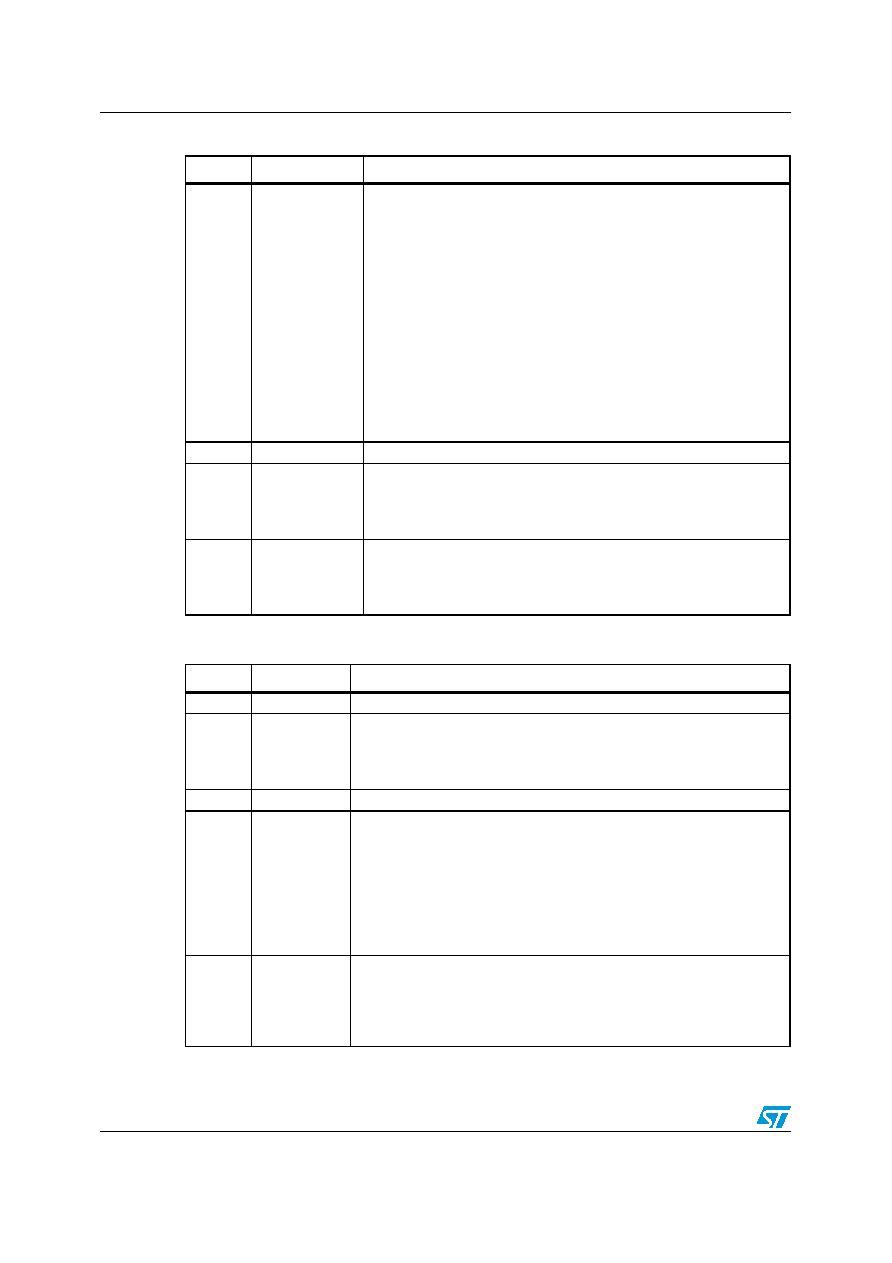
6:4
OSCRANGE[2:0]
Oscillator range
When the internal RC oscillator is not selected (option OSC = 1),
these option bits select the range of the resonator oscillator current
source or the external clock source.
000: Typ. frequency range with resonator (LP) = 1~2 MHz
001: Typ. frequency range with resonator (MP) = 2~4 MHz)
010: Typ. frequency range with resonator (MS) = 4~8 MHz)
011: Typ. frequency range with resonator (HS) = 8~16 MHz)
100: Typ. frequency range with resonator (VLP) = 32.768~ kHz)
101: External clock on OSC1
110: Reserved
111: External clock on PB4
Note: OSCRANGE[2:0] has no effect when AWUCK option is set to 0.
In this case, the VLP oscillator range is automatically selected
as AWU clock
3:2
-
Reserved, must be set to 1
1ROP_R
Readout protection for ROM
This option is for read protection of ROM
0: Readout protection off
1: Readout protection on
0ROP_D
Readout protection for data EEPROM
This option is for read protection of EEPROM memory.
0: Readout protection off
1: Readout protection on
Table 134.
Option byte 1 description
Bit
Bit name
Function
7
-
Reserved, must be set to 1(1)
6PLLOFF
PLL disable
This option bit enables or disables the PLL.
0: PLL enabled
1: PLL disabled (bypassed)
5
-
Reserved, must be set to 0(1)
4OSC
RC oscillator selection
This option bit enables selection of the internal RC oscillator.
0: RC oscillator on
1: RC oscillator off
Note: To improve clock stability and frequency accuracy when the RC
oscillator is selected, it is recommended to place a decoupling
capacitor, typically 100 nF, between the VDD and VSS pins as
close as possible to the ST7 device.
3:2
LVD[1:0]
Low voltage selection
These option bits enable the voltage detection block (LVD and AVD)
with a selected threshold to the LVD and AVD:
11: LVD off
10: LVD on (highest voltage threshold)
Table 133.
Option byte 0 description
Bit
Bit name
Function
相关PDF资料 |
PDF描述 |
|---|---|
| ST7FL38F2UAE | 8-BIT, FLASH, 8 MHz, MICROCONTROLLER, QCC20 |
| ST7L35MA/XXXR | 8-BIT, MROM, 8 MHz, MICROCONTROLLER, PDSO20 |
| ST7L35UA/XXXRS | 8-BIT, MROM, 8 MHz, MICROCONTROLLER, QCC20 |
| ST7L39UA/XXXE | 8-BIT, EEPROM, 8 MHz, MICROCONTROLLER, QCC20 |
| ST7PL35UA/XXXR | 8-BIT, MROM, 8 MHz, MICROCONTROLLER, QCC20 |
相关代理商/技术参数 |
参数描述 |
|---|---|
| ST7FL38F2MCE | 制造商:STMicroelectronics 功能描述: |
| ST7FL39F2MAE | 功能描述:8位微控制器 -MCU 8-bit MCU Automotive RoHS:否 制造商:Silicon Labs 核心:8051 处理器系列:C8051F39x 数据总线宽度:8 bit 最大时钟频率:50 MHz 程序存储器大小:16 KB 数据 RAM 大小:1 KB 片上 ADC:Yes 工作电源电压:1.8 V to 3.6 V 工作温度范围:- 40 C to + 105 C 封装 / 箱体:QFN-20 安装风格:SMD/SMT |
| ST7FL39F2MC | 制造商:STMicroelectronics 功能描述: |
| ST7FL39F2MCE | 制造商:STMicroelectronics 功能描述: |
| ST7FL39F2MCTR | 制造商:STMicroelectronics 功能描述: |
发布紧急采购,3分钟左右您将得到回复。