- 您现在的位置:买卖IC网 > PDF目录271213 > ST7FLITE19BF0B6 (STMICROELECTRONICS) 8-BIT, FLASH, 8 MHz, MICROCONTROLLER, PDIP20 PDF资料下载
参数资料
| 型号: | ST7FLITE19BF0B6 |
| 厂商: | STMICROELECTRONICS |
| 元件分类: | 微控制器/微处理器 |
| 英文描述: | 8-BIT, FLASH, 8 MHz, MICROCONTROLLER, PDIP20 |
| 封装: | 0.300 INCH, ROHS COMPLIANT, PLASTIC, DIP-20 |
| 文件页数: | 68/159页 |
| 文件大小: | 2855K |
| 代理商: | ST7FLITE19BF0B6 |
第1页第2页第3页第4页第5页第6页第7页第8页第9页第10页第11页第12页第13页第14页第15页第16页第17页第18页第19页第20页第21页第22页第23页第24页第25页第26页第27页第28页第29页第30页第31页第32页第33页第34页第35页第36页第37页第38页第39页第40页第41页第42页第43页第44页第45页第46页第47页第48页第49页第50页第51页第52页第53页第54页第55页第56页第57页第58页第59页第60页第61页第62页第63页第64页第65页第66页第67页当前第68页第69页第70页第71页第72页第73页第74页第75页第76页第77页第78页第79页第80页第81页第82页第83页第84页第85页第86页第87页第88页第89页第90页第91页第92页第93页第94页第95页第96页第97页第98页第99页第100页第101页第102页第103页第104页第105页第106页第107页第108页第109页第110页第111页第112页第113页第114页第115页第116页第117页第118页第119页第120页第121页第122页第123页第124页第125页第126页第127页第128页第129页第130页第131页第132页第133页第134页第135页第136页第137页第138页第139页第140页第141页第142页第143页第144页第145页第146页第147页第148页第149页第150页第151页第152页第153页第154页第155页第156页第157页第158页第159页
ST7LITE1xB
16/159
DATA EEPROM (Cont’d)
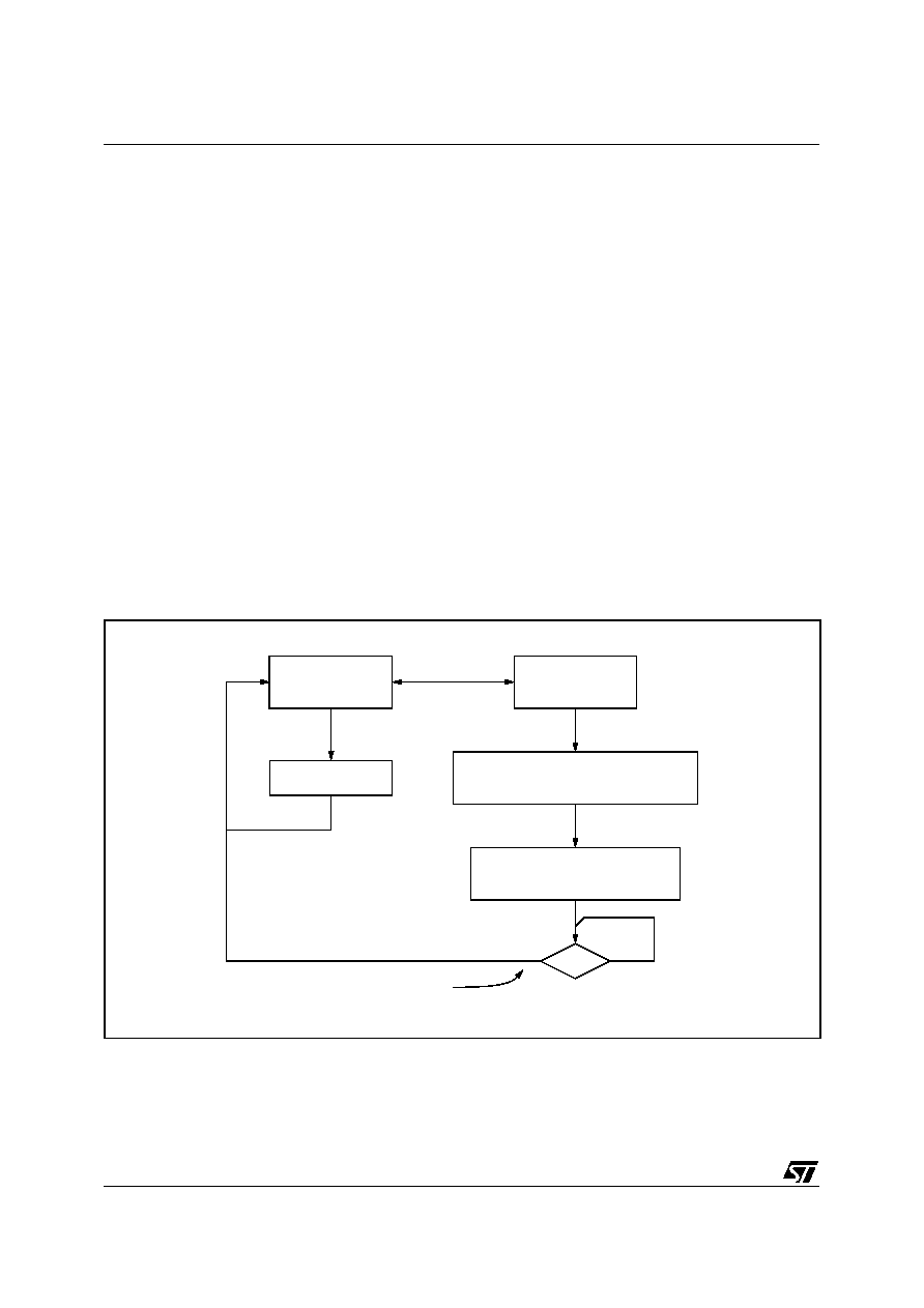
5.3 MEMORY ACCESS
The Data EEPROM memory read/write access
modes are controlled by the E2LAT bit of the EEP-
ROM Control/Status register (EECSR). The flow-
chart in Figure 8 describes these different memory
access modes.
Read Operation (E2LAT=0)
The EEPROM can be read as a normal ROM loca-
tion when the E2LAT bit of the EECSR register is
cleared.
On this device, Data EEPROM can also be used to
execute machine code. Take care not to write to
the Data EEPROM while executing from it. This
would result in an unexpected code being execut-
ed.
Write Operation (E2LAT=1)
To access the write mode, the E2LAT bit has to be
set by software (the E2PGM bit remains cleared).
When a write access to the EEPROM area occurs,
the value is latched inside the 32 data latches ac-
cording to its address.
When PGM bit is set by the software, all the previ-
ous bytes written in the data latches (up to 32) are
programmed in the EEPROM cells. The effective
high address (row) is determined by the last EEP-
ROM write sequence. To avoid wrong program-
ming, the user must take care that all the bytes
written between two programming sequences
have the same high address: only the five Least
Significant Bits of the address can change.
At the end of the programming cycle, the PGM and
LAT bits are cleared simultaneously.
Note: Care should be taken during the program-
ming cycle. Writing to the same memory location
will over-program the memory (logical AND be-
tween the two write access data result) because
the data latches are only cleared at the end of the
programming cycle and by the falling edge of the
E2LAT bit.
It is not possible to read the latched data.
This note is illustrated by the Figure 10.
Figure 8. Data EEPROM Programming Flowchart
READ MODE
E2LAT=0
E2PGM=0
WRITE MODE
E2LAT=1
E2PGM=0
READ BYTES
IN EEPROM AREA
WRITE UP TO 32 BYTES
IN EEPROM AREA
(with the same 11 MSB of the address)
START PROGRAMMING CYCLE
E2LAT=1
E2PGM=1 (set by software)
E2LAT
01
CLEARED BY HARDWARE
1
相关PDF资料 |
PDF描述 |
|---|---|
| ST7PLITE15BF0B3 | 8-BIT, MROM, 8 MHz, MICROCONTROLLER, PDIP20 |
| STR711FR0H3 | 32-BIT, FLASH, 66 MHz, RISC MICROCONTROLLER, PBGA64 |
| STR711FRH3 | 32-BIT, FLASH, 66 MHz, RISC MICROCONTROLLER, PBGA64 |
| STR711FZ2H3TR | 32-BIT, FLASH, 66 MHz, RISC MICROCONTROLLER, PBGA144 |
| STR711FZT1TR | 32-BIT, FLASH, 66 MHz, RISC MICROCONTROLLER, PQFP144 |
相关代理商/技术参数 |
参数描述 |
|---|---|
| ST7FLITE19F1B6 | 功能描述:8位微控制器 -MCU Flash 4K SPI RoHS:否 制造商:Silicon Labs 核心:8051 处理器系列:C8051F39x 数据总线宽度:8 bit 最大时钟频率:50 MHz 程序存储器大小:16 KB 数据 RAM 大小:1 KB 片上 ADC:Yes 工作电源电压:1.8 V to 3.6 V 工作温度范围:- 40 C to + 105 C 封装 / 箱体:QFN-20 安装风格:SMD/SMT |
| ST7FLITE19F1B6 | 制造商:STMicroelectronics 功能描述:IC 8BIT FLASH MCU 7FLITE19 DIP20 |
| ST7FLITE19F1M6 | 功能描述:8位微控制器 -MCU Flash 4K SPI RoHS:否 制造商:Silicon Labs 核心:8051 处理器系列:C8051F39x 数据总线宽度:8 bit 最大时钟频率:50 MHz 程序存储器大小:16 KB 数据 RAM 大小:1 KB 片上 ADC:Yes 工作电源电压:1.8 V to 3.6 V 工作温度范围:- 40 C to + 105 C 封装 / 箱体:QFN-20 安装风格:SMD/SMT |
| ST7FLITE20F1B6 | 功能描述:8位微控制器 -MCU 8 BITS MICROCONTR RoHS:否 制造商:Silicon Labs 核心:8051 处理器系列:C8051F39x 数据总线宽度:8 bit 最大时钟频率:50 MHz 程序存储器大小:16 KB 数据 RAM 大小:1 KB 片上 ADC:Yes 工作电源电压:1.8 V to 3.6 V 工作温度范围:- 40 C to + 105 C 封装 / 箱体:QFN-20 安装风格:SMD/SMT |
| ST7FLITE20F2B6 | 功能描述:8位微控制器 -MCU Flash 8K SPI 384 RAM RoHS:否 制造商:Silicon Labs 核心:8051 处理器系列:C8051F39x 数据总线宽度:8 bit 最大时钟频率:50 MHz 程序存储器大小:16 KB 数据 RAM 大小:1 KB 片上 ADC:Yes 工作电源电压:1.8 V to 3.6 V 工作温度范围:- 40 C to + 105 C 封装 / 箱体:QFN-20 安装风格:SMD/SMT |
发布紧急采购,3分钟左右您将得到回复。