- 您现在的位置:买卖IC网 > PDF目录69380 > ST92T196A9 (STMICROELECTRONICS) 16-BIT, OTPROM, 24 MHz, MICROCONTROLLER, PDIP56 PDF资料下载
参数资料
| 型号: | ST92T196A9 |
| 厂商: | STMICROELECTRONICS |
| 元件分类: | 微控制器/微处理器 |
| 英文描述: | 16-BIT, OTPROM, 24 MHz, MICROCONTROLLER, PDIP56 |
| 封装: | 0.600 INCH, PLASTIC, SDIP-56 |
| 文件页数: | 134/268页 |
| 文件大小: | 3049K |
| 代理商: | ST92T196A9 |
第1页第2页第3页第4页第5页第6页第7页第8页第9页第10页第11页第12页第13页第14页第15页第16页第17页第18页第19页第20页第21页第22页第23页第24页第25页第26页第27页第28页第29页第30页第31页第32页第33页第34页第35页第36页第37页第38页第39页第40页第41页第42页第43页第44页第45页第46页第47页第48页第49页第50页第51页第52页第53页第54页第55页第56页第57页第58页第59页第60页第61页第62页第63页第64页第65页第66页第67页第68页第69页第70页第71页第72页第73页第74页第75页第76页第77页第78页第79页第80页第81页第82页第83页第84页第85页第86页第87页第88页第89页第90页第91页第92页第93页第94页第95页第96页第97页第98页第99页第100页第101页第102页第103页第104页第105页第106页第107页第108页第109页第110页第111页第112页第113页第114页第115页第116页第117页第118页第119页第120页第121页第122页第123页第124页第125页第126页第127页第128页第129页第130页第131页第132页第133页当前第134页第135页第136页第137页第138页第139页第140页第141页第142页第143页第144页第145页第146页第147页第148页第149页第150页第151页第152页第153页第154页第155页第156页第157页第158页第159页第160页第161页第162页第163页第164页第165页第166页第167页第168页第169页第170页第171页第172页第173页第174页第175页第176页第177页第178页第179页第180页第181页第182页第183页第184页第185页第186页第187页第188页第189页第190页第191页第192页第193页第194页第195页第196页第197页第198页第199页第200页第201页第202页第203页第204页第205页第206页第207页第208页第209页第210页第211页第212页第213页第214页第215页第216页第217页第218页第219页第220页第221页第222页第223页第224页第225页第226页第227页第228页第229页第230页第231页第232页第233页第234页第235页第236页第237页第238页第239页第240页第241页第242页第243页第244页第245页第246页第247页第248页第249页第250页第251页第252页第253页第254页第255页第256页第257页第258页第259页第260页第261页第262页第263页第264页第265页第266页第267页第268页
219/268
- A/D CONVERTER (A/D)
8.14 A/D CONVERTER (A/D)
8.14.1 Introduction
The 8 bit Analog to Digital Converter uses a fully
differential analog configuration for the best noise
immunity and precision performance. The analog
voltage references of the converter are connected
to the internal AVDD & AVSS analog supply pins of
the chip if they are available, otherwise to the ordi-
nary VDD and VSS supply pins of the chip. The
guaranteed accuracy depends on the device (see
Electrical Characteristics). A fast Sample/Hold al-
lows quick signal sampling for minimum warping
effect and conversion error.
8.14.2 Main Features
s
8-bit resolution A/D Converter
s
Single Conversion Time (including Sampling
Time):
– 138 internal system clock periods in slow
mode (~5.6 s @25Mhz internal system
clock);
– 78 INTCLK periods in fast mode (~6.5 s @
12MHZ internal system clock)
s
Sample/Hold: Tsample=
– 84 INTCLK periods in slow mode (~3.4 s
@25Mhz internal system clock)
– 48 INTCLK periods in fast mode (~4 s
@12Mhz internal system clock)
s
Up to 8 Analog Inputs (the number of inputs is
device dependent, see device pinout)
s
Single/Continuous Conversion Mode
s
External
source
Trigger
(Alternate
synchronization)
s
Power Down mode (Zero Power Consumption)
s
1 Control Logic Register
s
1 Data Register
8.14.3 General Description
Depending on the device, up to 8 analog inputs
can be selected by software.
Different conversion modes are provided: single,
continuous, or triggered. The continuous mode
performs a continuous conversion flow of the se-
lected channel, while in the single mode the se-
lected channel is converted once and then the log-
ic waits for a new hardware or software restart.
A data register (ADDTR) is available, mapped in
page 62, allowing data storage (in single or contin-
uous mode).
The start conversion event can be managed either
– by software, writing the START/STOP bit of the
Control Logic Register
– or by hardware using an external signal on the
EXTRG triggered input (negative edge sensitive)
connected as an Alternate Function to an I/O port
bit
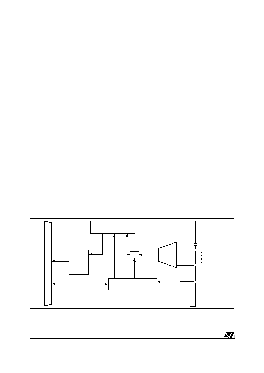
Figure 98. A/D Converter Block Diagram
n
ST
9
BU
S
SUCCESSIVE
APPROXIMATION
REGISTER
ANALOG
MUX
DATA
REGISTER
CONTROL LOGIC
S/H
Ain1
Ainx
Ain0
EXTRG
相关PDF资料 |
PDF描述 |
|---|---|
| ST92E196A9 | 16-BIT, EEPROM, 24 MHz, MICROCONTROLLER, CDIP56 |
| ST92T196B7 | 16-BIT, OTPROM, 24 MHz, MICROCONTROLLER, PDIP56 |
| STA2051TR | 32-BIT, FLASH, 66 MHz, RISC MICROCONTROLLER, PQFP64 |
| STA2051ETR | 32-BIT, FLASH, 66 MHz, RISC MICROCONTROLLER, PQFP64 |
| STA2051 | 32-BIT, FLASH, 66 MHz, RISC MICROCONTROLLER, PQFP64 |
相关代理商/技术参数 |
参数描述 |
|---|---|
| ST92T96N9B1/AIN | 制造商:STMicroelectronics 功能描述: |
| ST-930 | 制造商:UNBRANDED 功能描述:MULTIMETER DIGITAL BARGRAPH |
| ST93003 | 功能描述:两极晶体管 - BJT Hi Vltg FAST SWITCH PNP Pwr TRANSISTOR RoHS:否 制造商:STMicroelectronics 配置: 晶体管极性:PNP 集电极—基极电压 VCBO: 集电极—发射极最大电压 VCEO:- 40 V 发射极 - 基极电压 VEBO:- 6 V 集电极—射极饱和电压: 最大直流电集电极电流: 增益带宽产品fT: 直流集电极/Base Gain hfe Min:100 A 最大工作温度: 安装风格:SMD/SMT 封装 / 箱体:PowerFLAT 2 x 2 |
| ST9300403SS | 制造商:Seagate Technology 功能描述:- Bulk |
| ST9300453SS | 制造商:Seagate Technology 功能描述:- Bulk |
发布紧急采购,3分钟左右您将得到回复。