- 您现在的位置:买卖IC网 > PDF目录98221 > THS3111CDGNG4 (TEXAS INSTRUMENTS INC) 1 CHANNEL, VIDEO AMPLIFIER, PDSO8 PDF资料下载
参数资料
| 型号: | THS3111CDGNG4 |
| 厂商: | TEXAS INSTRUMENTS INC |
| 元件分类: | 音频/视频放大 |
| 英文描述: | 1 CHANNEL, VIDEO AMPLIFIER, PDSO8 |
| 封装: | GREEN, PLASTIC, MSOP-8 |
| 文件页数: | 10/36页 |
| 文件大小: | 995K |
| 代理商: | THS3111CDGNG4 |
第1页第2页第3页第4页第5页第6页第7页第8页第9页当前第10页第11页第12页第13页第14页第15页第16页第17页第18页第19页第20页第21页第22页第23页第24页第25页第26页第27页第28页第29页第30页第31页第32页第33页第34页第35页第36页
_
+
VS
-VS
49.9
806
Ferrite Bead
1
F
200
VS
100
LOAD
0
10
20
30
40
50
60
10
100
CL - Capacitive Load - pF
Recommended
R
Gain = 5,
RL = 100 ,
VS = ±15 V
ISO
-
_
+
VS
-VS
49.9
806
5.11
1
F
200
VS
100
LOAD
RISO
_
+
VS
-VS
49.9
5.11
1
F
200
VS
27 pF
806
RF
RG
750
100
LOAD
RIN
SLOS422E – SEPTEMBER 2003 – REVISED OCTOBER 2009........................................................................................................................................ www.ti.com
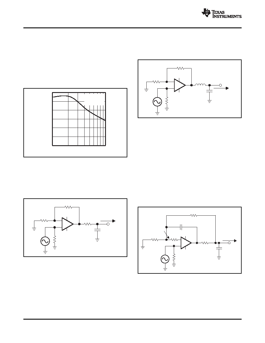
Driving Capacitive Loads
frequency load independence of the amplifier while
isolating the phase shift caused by the capacitance at
Applications such as FET drivers and line drivers can
high frequency. Use a ferrite chip with similar
be highly capacitive and cause stability problems for
impedance to RISO, 20 to 50 , at 100 MHz and
high-speed amplifiers.
low impedance at dc.
methods for driving capacitive loads. The basic idea
is to use a resistor or ferrite chip to isolate the phase
shift at high frequency caused by the capacitive load
from the amplifier feedback path. See Figure 55 for
recommended resistor values versus capacitive load.
Figure 57. Ferrite Bead to Isolate Capacitive Load
Figure 58 shows another method used to maintain
the low frequency load independence of the amplifier
while isolating the phase shift caused by the
capacitance at high frequency. At low frequency,
feedback is mainly from the load side of RISO. At high
frequency, the feedback is mainly via the 27-pF
Figure 55. Recommended RISO vs Capacitive
capacitor. The resistor RIN in series with the negative
Load
input is used to stabilize the amplifier and should be
equal to the recommended value of RF at unity gain.
Replacing RIN with a ferrite of similar impedance at
Placing a small series resistor, RISO, between the
about 100 MHz as shown in Figure 59 gives similar
amplifier output and the capacitive load, as shown in
results with reduced dc offset and low frequency
Figure 56, is an easy way of isolating the load
noise. (See the Additional Reference Material section
capacitance.
for
expanding
the
usability
of
current-feedback
amplifiers.)
Figure 56. Resistor to Isolate Capacitive Load
Using a ferrite chip in place of RISO, as shown in
Figure 57, is another approach of isolating the output
Figure 58. Feedback Technique with Input
of the amplifier. The ferrite impedance characteristic
Resistor for Capacitive Load
versus frequency is useful to maintain the low
18
Copyright 2003–2009, Texas Instruments Incorporated
相关PDF资料 |
PDF描述 |
|---|---|
| THS3110CDGN | 1 CHANNEL, VIDEO AMPLIFIER, PDSO8 |
| THS3110CDGNR | 1 CHANNEL, VIDEO AMPLIFIER, PDSO8 |
| THS3111CDGNR | 1 CHANNEL, VIDEO AMPLIFIER, PDSO8 |
| THS3111CDR | 1 CHANNEL, VIDEO AMPLIFIER, PDSO8 |
| THS3111CD | 1 CHANNEL, VIDEO AMPLIFIER, PDSO8 |
相关代理商/技术参数 |
参数描述 |
|---|---|
| THS3111CDGNR | 功能描述:高速运算放大器 Single Lo-Noise Hi-Vltg Crnt-Feedbck RoHS:否 制造商:Texas Instruments 通道数量:1 电压增益 dB:116 dB 输入补偿电压:0.5 mV 转换速度:55 V/us 工作电源电压:36 V 电源电流:7.5 mA 最大工作温度:+ 85 C 安装风格:SMD/SMT 封装 / 箱体:SOIC-8 封装:Tube |
| THS3111CDGNRG4 | 功能描述:高速运算放大器 Single Lo-Noise Hi-Vltg Crnt-Feedbck RoHS:否 制造商:Texas Instruments 通道数量:1 电压增益 dB:116 dB 输入补偿电压:0.5 mV 转换速度:55 V/us 工作电源电压:36 V 电源电流:7.5 mA 最大工作温度:+ 85 C 安装风格:SMD/SMT 封装 / 箱体:SOIC-8 封装:Tube |
| THS3111CDR | 功能描述:高速运算放大器 Single Lo-Noise Hi-Vltg Crnt-Feedbck RoHS:否 制造商:Texas Instruments 通道数量:1 电压增益 dB:116 dB 输入补偿电压:0.5 mV 转换速度:55 V/us 工作电源电压:36 V 电源电流:7.5 mA 最大工作温度:+ 85 C 安装风格:SMD/SMT 封装 / 箱体:SOIC-8 封装:Tube |
| THS3111CDRG4 | 功能描述:高速运算放大器 Single Lo-Noise Hi-Vltg Crnt-Feedbck RoHS:否 制造商:Texas Instruments 通道数量:1 电压增益 dB:116 dB 输入补偿电压:0.5 mV 转换速度:55 V/us 工作电源电压:36 V 电源电流:7.5 mA 最大工作温度:+ 85 C 安装风格:SMD/SMT 封装 / 箱体:SOIC-8 封装:Tube |
| THS3111EVM | 功能描述:放大器 IC 开发工具 THS3111 Eval Mod RoHS:否 制造商:International Rectifier 产品:Demonstration Boards 类型:Power Amplifiers 工具用于评估:IR4302 工作电源电压:13 V to 23 V |
发布紧急采购,3分钟左右您将得到回复。