- 您现在的位置:买卖IC网 > PDF目录98221 > THS3111CDGNG4 (TEXAS INSTRUMENTS INC) 1 CHANNEL, VIDEO AMPLIFIER, PDSO8 PDF资料下载
参数资料
| 型号: | THS3111CDGNG4 |
| 厂商: | TEXAS INSTRUMENTS INC |
| 元件分类: | 音频/视频放大 |
| 英文描述: | 1 CHANNEL, VIDEO AMPLIFIER, PDSO8 |
| 封装: | GREEN, PLASTIC, MSOP-8 |
| 文件页数: | 8/36页 |
| 文件大小: | 995K |
| 代理商: | THS3111CDGNG4 |
第1页第2页第3页第4页第5页第6页第7页当前第8页第9页第10页第11页第12页第13页第14页第15页第16页第17页第18页第19页第20页第21页第22页第23页第24页第25页第26页第27页第28页第29页第30页第31页第32页第33页第34页第35页第36页
_
+
THS3110
RF
1 k
49.9
0.1
F
6.8
F
-VS
-15 V
RG
50
Source
+
VI
0.1
F
6.8
F
+
+VS
15 V
49.9
50
LOAD
1 k
SLOS422E – SEPTEMBER 2003 – REVISED OCTOBER 2009........................................................................................................................................ www.ti.com
APPLICATION INFORMATION
MAXIMUM SLEW RATE FOR REPETITIVE
SIGNALS
The THS3110 and THS3111 are recommended for
high slew rate pulsed applications where the internal
nodes of the amplifier have time to stabilize between
pulses. It is recommended to have at least 20-ns
delay between pulses.
The THS3110 and THS3111 are not recommended
for applications with repetitive signals (sine, square,
sawtooth, or other) that exceed 900 V/
μs. Using the
part in these applications results in excessive current
draw from the power supply and possible device
damage.
For applications with high slew rate, repetitive signals,
THS3096 (dual) are recommended.
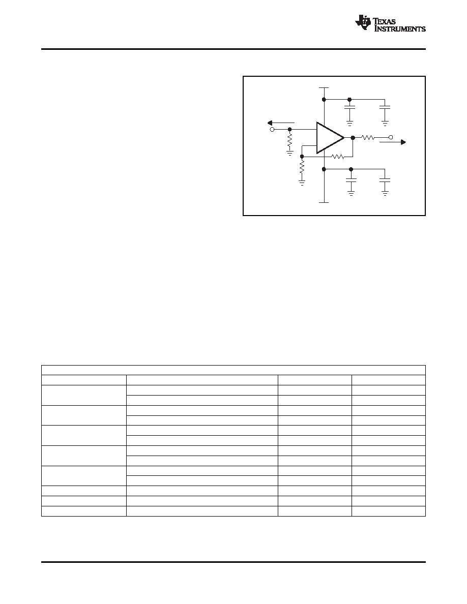
Figure 51. Wideband, Noninverting Gain
Configuration
WIDEBAND, NONINVERTING OPERATION
The THS3110 and THS3111 are unity-gain stable,
Current-feedback amplifiers are highly dependent on
100-MHz, current-feedback operational amplifiers,
the feedback resistor RF for maximum performance
designed to operate from a ±5-V to ±15-V power
and stability. Table 1 shows the optimal gain setting
supply.
resistors RF and RG at different gains to give
maximum bandwidth with minimal peaking in the
Figure 51 shows the THS3111 in a noninverting gain
frequency response. Higher bandwidths can be
of 2-V/V configuration typically used to generate the
achieved, at the expense of added peaking in the
performance
curves.
Most
of
the
curves
were
frequency response, by using even lower values for
characterized using signal sources with 50-
source
RF.
Conversely,
increasing
RF
decreases
the
impedance,
and
with
measurement
equipment
bandwidth, but stability is improved.
presenting a 50-
load impedance.
Table 1. Recommended Resistor Values for
Optimum Frequency Response
THS3110 AND THS3111 RF AND RG VALUES FOR MINIMAL PEAKING WITH RL = 100
GAIN (V/V)
SUPPLY VOLTAGE (V)
RG ()
RF ()
±15
—
1.5 k
1
±5
—
1.5 k
±15
1 k
2
±5
1.15 k
±15
200
806
5
±5
200
806
±15
66.5
604
10
±5
66.5
604
±15
1 k
–1
±5
1 k
–2
±15 and ±5
549
1.1 k
–5
±15 and ±5
182
909
–10
±15 and ±5
64.9
649
16
Copyright 2003–2009, Texas Instruments Incorporated
相关PDF资料 |
PDF描述 |
|---|---|
| THS3110CDGN | 1 CHANNEL, VIDEO AMPLIFIER, PDSO8 |
| THS3110CDGNR | 1 CHANNEL, VIDEO AMPLIFIER, PDSO8 |
| THS3111CDGNR | 1 CHANNEL, VIDEO AMPLIFIER, PDSO8 |
| THS3111CDR | 1 CHANNEL, VIDEO AMPLIFIER, PDSO8 |
| THS3111CD | 1 CHANNEL, VIDEO AMPLIFIER, PDSO8 |
相关代理商/技术参数 |
参数描述 |
|---|---|
| THS3111CDGNR | 功能描述:高速运算放大器 Single Lo-Noise Hi-Vltg Crnt-Feedbck RoHS:否 制造商:Texas Instruments 通道数量:1 电压增益 dB:116 dB 输入补偿电压:0.5 mV 转换速度:55 V/us 工作电源电压:36 V 电源电流:7.5 mA 最大工作温度:+ 85 C 安装风格:SMD/SMT 封装 / 箱体:SOIC-8 封装:Tube |
| THS3111CDGNRG4 | 功能描述:高速运算放大器 Single Lo-Noise Hi-Vltg Crnt-Feedbck RoHS:否 制造商:Texas Instruments 通道数量:1 电压增益 dB:116 dB 输入补偿电压:0.5 mV 转换速度:55 V/us 工作电源电压:36 V 电源电流:7.5 mA 最大工作温度:+ 85 C 安装风格:SMD/SMT 封装 / 箱体:SOIC-8 封装:Tube |
| THS3111CDR | 功能描述:高速运算放大器 Single Lo-Noise Hi-Vltg Crnt-Feedbck RoHS:否 制造商:Texas Instruments 通道数量:1 电压增益 dB:116 dB 输入补偿电压:0.5 mV 转换速度:55 V/us 工作电源电压:36 V 电源电流:7.5 mA 最大工作温度:+ 85 C 安装风格:SMD/SMT 封装 / 箱体:SOIC-8 封装:Tube |
| THS3111CDRG4 | 功能描述:高速运算放大器 Single Lo-Noise Hi-Vltg Crnt-Feedbck RoHS:否 制造商:Texas Instruments 通道数量:1 电压增益 dB:116 dB 输入补偿电压:0.5 mV 转换速度:55 V/us 工作电源电压:36 V 电源电流:7.5 mA 最大工作温度:+ 85 C 安装风格:SMD/SMT 封装 / 箱体:SOIC-8 封装:Tube |
| THS3111EVM | 功能描述:放大器 IC 开发工具 THS3111 Eval Mod RoHS:否 制造商:International Rectifier 产品:Demonstration Boards 类型:Power Amplifiers 工具用于评估:IR4302 工作电源电压:13 V to 23 V |
发布紧急采购,3分钟左右您将得到回复。