- 您现在的位置:买卖IC网 > PDF目录98221 > THS3111CDGNG4 (TEXAS INSTRUMENTS INC) 1 CHANNEL, VIDEO AMPLIFIER, PDSO8 PDF资料下载
参数资料
| 型号: | THS3111CDGNG4 |
| 厂商: | TEXAS INSTRUMENTS INC |
| 元件分类: | 音频/视频放大 |
| 英文描述: | 1 CHANNEL, VIDEO AMPLIFIER, PDSO8 |
| 封装: | GREEN, PLASTIC, MSOP-8 |
| 文件页数: | 13/36页 |
| 文件大小: | 995K |
| 代理商: | THS3111CDGNG4 |
第1页第2页第3页第4页第5页第6页第7页第8页第9页第10页第11页第12页当前第13页第14页第15页第16页第17页第18页第19页第20页第21页第22页第23页第24页第25页第26页第27页第28页第29页第30页第31页第32页第33页第34页第35页第36页
0
200
400
600
800
1000
1200
1400
1600
1800
2000
100 k
1 M
10 M
100 M
1 G
f - Frequency - Hz
Powerdown
Output
Impedance
-
Gain = 2
RF = 1 k
VS = ±15 V and ±5 V
SLOS422E – SEPTEMBER 2003 – REVISED OCTOBER 2009........................................................................................................................................ www.ti.com
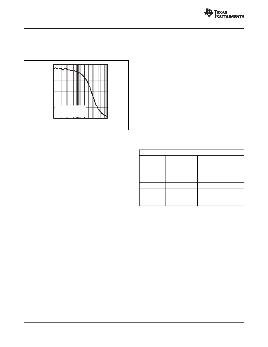
Figure 62 shows the total system output impedance
POWER-DOWN REFERENCE PIN
which includes the amplifier output impedance in
OPERATION
parallel with the feedback plus gain resistors, which
In addition to the power-down pin, the THS3110
cumulate to 1870
. Figure 51 shows this circuit
features a reference pin (REF) which allows the user
configuration for reference.
to control the enable or disable power-down voltage
levels applied to the PD pin. In most split-supply
applications, the reference pin is connected to
ground. In either case, the user needs to be aware of
voltage-level thresholds that apply to the power-down
pin. The tables below show examples and illustrate
the relationship between the reference voltage and
the power-down thresholds. In the table, the threshold
levels are derived by the following equations:
PD
≤ REF + 0.8 V for enable
PD
≥ REF + 2.0 V for disable
where the usable range at the REF pin is
VS– ≤ VREF ≤ (VS+ – 4 V).
The recommended mode of operation is to tie the
REF pin to midrail, thus setting the enable/disable
Figure 62. Power-Down Output Impedance vs
thresholds to Vmidrail + 0.8 V and Vmidrail + 2 V
Frequency
respectively.
As with most current feedback amplifiers, the internal
POWER-DOWN THRESHOLD VOLTAGE LEVELS
architecture places some limitations on the system
SUPPLY
REFERENCE PIN
ENABLE
DISABLE
when in power-down mode. Most notably is the fact
VOLTAGE (V)
LEVEL (V)
that the amplifier actually turns ON if there is a ±0.7 V
±15, ±5
0.0
0.8
2.0
or greater difference between the two input nodes
±15
2.0
2.8
4
(V+ and V–) of the amplifier. If this difference
±15
–2.0
–1.2
0
exceeds ±0.7 V, the output of the amplifier creates an
±5
1.0
1.8
3
output voltage equal to approximately [(V+ – V–) –
0.7 V] × Gain. Also, if a voltage is applied to the
±5
–1.0
–0.2
1
output while in power-down mode, the V– node
+30
15
15.8
17
voltage is equal to VO(applied) × RG/(RF + RG). For low
+10
5.0
5.8
7
gain configurations and a large applied voltage at the
output, the amplifier may actually turn ON due to the
Note that if the REF pin is left unterminated, it floats
aforementioned behavior.
to
the
positive
rail
and
falls
outside
of
the
recommended operating range given above (VS– ≤
The time delays associated with turning the device on
VREF ≤ VS+ – 4 V). As a result, it no longer serves as
and off are specified as the time it takes for the
a
reliable
reference
for
the
PD
pin
and
the
amplifier to reach either 10% or 90% of the final
enable/disable thresholds given above no longer
output voltage. The time delays are in the order of
apply. If the PD pin is also left unterminated, it also
microseconds because the amplifier moves in and out
floats to the positive rail and the device is disabled. If
of the linear mode of operation in these transitions.
balanced, split supplies are used (±VS) and the REF
and PD pins are grounded, the device is enabled.
20
Copyright 2003–2009, Texas Instruments Incorporated
相关PDF资料 |
PDF描述 |
|---|---|
| THS3110CDGN | 1 CHANNEL, VIDEO AMPLIFIER, PDSO8 |
| THS3110CDGNR | 1 CHANNEL, VIDEO AMPLIFIER, PDSO8 |
| THS3111CDGNR | 1 CHANNEL, VIDEO AMPLIFIER, PDSO8 |
| THS3111CDR | 1 CHANNEL, VIDEO AMPLIFIER, PDSO8 |
| THS3111CD | 1 CHANNEL, VIDEO AMPLIFIER, PDSO8 |
相关代理商/技术参数 |
参数描述 |
|---|---|
| THS3111CDGNR | 功能描述:高速运算放大器 Single Lo-Noise Hi-Vltg Crnt-Feedbck RoHS:否 制造商:Texas Instruments 通道数量:1 电压增益 dB:116 dB 输入补偿电压:0.5 mV 转换速度:55 V/us 工作电源电压:36 V 电源电流:7.5 mA 最大工作温度:+ 85 C 安装风格:SMD/SMT 封装 / 箱体:SOIC-8 封装:Tube |
| THS3111CDGNRG4 | 功能描述:高速运算放大器 Single Lo-Noise Hi-Vltg Crnt-Feedbck RoHS:否 制造商:Texas Instruments 通道数量:1 电压增益 dB:116 dB 输入补偿电压:0.5 mV 转换速度:55 V/us 工作电源电压:36 V 电源电流:7.5 mA 最大工作温度:+ 85 C 安装风格:SMD/SMT 封装 / 箱体:SOIC-8 封装:Tube |
| THS3111CDR | 功能描述:高速运算放大器 Single Lo-Noise Hi-Vltg Crnt-Feedbck RoHS:否 制造商:Texas Instruments 通道数量:1 电压增益 dB:116 dB 输入补偿电压:0.5 mV 转换速度:55 V/us 工作电源电压:36 V 电源电流:7.5 mA 最大工作温度:+ 85 C 安装风格:SMD/SMT 封装 / 箱体:SOIC-8 封装:Tube |
| THS3111CDRG4 | 功能描述:高速运算放大器 Single Lo-Noise Hi-Vltg Crnt-Feedbck RoHS:否 制造商:Texas Instruments 通道数量:1 电压增益 dB:116 dB 输入补偿电压:0.5 mV 转换速度:55 V/us 工作电源电压:36 V 电源电流:7.5 mA 最大工作温度:+ 85 C 安装风格:SMD/SMT 封装 / 箱体:SOIC-8 封装:Tube |
| THS3111EVM | 功能描述:放大器 IC 开发工具 THS3111 Eval Mod RoHS:否 制造商:International Rectifier 产品:Demonstration Boards 类型:Power Amplifiers 工具用于评估:IR4302 工作电源电压:13 V to 23 V |
发布紧急采购,3分钟左右您将得到回复。