- 您现在的位置:买卖IC网 > PDF目录98221 > THS3111CDGNG4 (TEXAS INSTRUMENTS INC) 1 CHANNEL, VIDEO AMPLIFIER, PDSO8 PDF资料下载
参数资料
| 型号: | THS3111CDGNG4 |
| 厂商: | TEXAS INSTRUMENTS INC |
| 元件分类: | 音频/视频放大 |
| 英文描述: | 1 CHANNEL, VIDEO AMPLIFIER, PDSO8 |
| 封装: | GREEN, PLASTIC, MSOP-8 |
| 文件页数: | 15/36页 |
| 文件大小: | 995K |
| 代理商: | THS3111CDGNG4 |
第1页第2页第3页第4页第5页第6页第7页第8页第9页第10页第11页第12页第13页第14页当前第15页第16页第17页第18页第19页第20页第21页第22页第23页第24页第25页第26页第27页第28页第29页第30页第31页第32页第33页第34页第35页第36页
0.205
(5,21)
0.060
(1,52)
0.013
(0,33)
0.017
(0,432)
0.025
(0,64)
0.094
(2,39)
0.040
(1,01)
0.035
(0,89)
0.030
(0,76)
0.075
(1,91)
0.010
vias
(0,254)
DIE
Side View (a)
DIE
End View (b)
Thermal
Pad
Bottom View (c)
SLOS422E – SEPTEMBER 2003 – REVISED OCTOBER 2009........................................................................................................................................ www.ti.com
PowerPAD DESIGN CONSIDERATIONS
PowerPAD LAYOUT CONSIDERATIONS
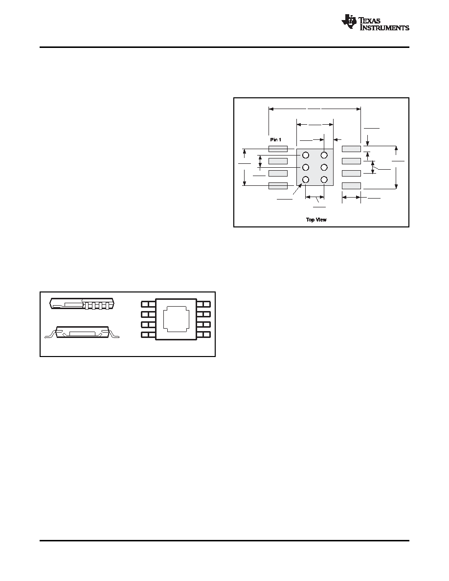
1. PCB with a top side etch pattern as shown in
The THS3110 and THS3111 are available in a
Figure 64. There should be etch for the leads as
thermally-enhanced PowerPAD family of packages.
well as etch for the thermal pad.
These packages are constructed using a downset
leadframe upon which the die is mounted (see
Figure 63a and Figure 63b). This arrangement results
in the lead frame being exposed as a thermal pad on
the underside of the package (see Figure 63c).
Because this thermal pad has direct thermal contact
with the die, excellent thermal performance can be
achieved by providing a good thermal path away from
the thermal pad. Note that devices such as the
THS311x have no electrical connection between the
PowerPAD and the die.
The PowerPAD package allows for both assembly
and thermal management in one manufacturing
operation. During the surface-mount solder operation
(when the leads are being soldered), the thermal pad
can also be soldered to a copper area underneath the
package. Through the use of thermal paths within this
copper area, heat can be conducted away from the
Dimensions are in inches (mm).
package into either a ground plane or other heat
dissipating device.
Figure 64. DGN PowerPAD PCB Etch and
Via Pattern
The PowerPAD package represents a breakthrough
in combining the small area and ease of assembly of
2. Place five holes in the area of the thermal pad.
surface
mount
with
the,
heretofore,
awkward
These holes should be 0.01 inch (0,254 mm) in
mechanical methods of heatsinking.
diameter. Keep them small so that solder wicking
through the holes is not a problem during reflow.
3. Additional vias may be placed anywhere along
the thermal plane outside of the thermal pad
area. This helps dissipate the heat generated by
the THS3110/THS3111 IC. These additional vias
may be larger than the 0.01-inch (0,254 mm)
diameter vias directly under the thermal pad.
They can be larger because they are not in the
thermal pad area to be soldered so that wicking
Figure 63. Views of Thermal Enhanced Package
is not a problem.
4. Connect all holes to the internal ground plane.
Although there are many ways to properly heatsink
Note that the PowerPAD is electrically isolated
the PowerPAD package, the following steps illustrate
from the silicon and all leads. Connecting the
the recommended approach.
PowerPAD to any potential voltage such as VS–,
is acceptable as there is no electrical connection
space
to the silicon.
space
5. When connecting these holes to the ground
plane, do not use the typical web or spoke via
space
connection methodology. Web connections have
space
a high thermal resistance connection that is
useful for slowing the heat transfer during
space
soldering operations. This makes the soldering of
space
vias that have plane connections easier. In this
application, however, low thermal resistance is
space
desired for the most efficient heat transfer.
space
Therefore,
the
holes
under
the
THS3110/THS3111 PowerPAD package should
space
make their connection to the internal ground
plane with a complete connection around the
space
22
Copyright 2003–2009, Texas Instruments Incorporated
相关PDF资料 |
PDF描述 |
|---|---|
| THS3110CDGN | 1 CHANNEL, VIDEO AMPLIFIER, PDSO8 |
| THS3110CDGNR | 1 CHANNEL, VIDEO AMPLIFIER, PDSO8 |
| THS3111CDGNR | 1 CHANNEL, VIDEO AMPLIFIER, PDSO8 |
| THS3111CDR | 1 CHANNEL, VIDEO AMPLIFIER, PDSO8 |
| THS3111CD | 1 CHANNEL, VIDEO AMPLIFIER, PDSO8 |
相关代理商/技术参数 |
参数描述 |
|---|---|
| THS3111CDGNR | 功能描述:高速运算放大器 Single Lo-Noise Hi-Vltg Crnt-Feedbck RoHS:否 制造商:Texas Instruments 通道数量:1 电压增益 dB:116 dB 输入补偿电压:0.5 mV 转换速度:55 V/us 工作电源电压:36 V 电源电流:7.5 mA 最大工作温度:+ 85 C 安装风格:SMD/SMT 封装 / 箱体:SOIC-8 封装:Tube |
| THS3111CDGNRG4 | 功能描述:高速运算放大器 Single Lo-Noise Hi-Vltg Crnt-Feedbck RoHS:否 制造商:Texas Instruments 通道数量:1 电压增益 dB:116 dB 输入补偿电压:0.5 mV 转换速度:55 V/us 工作电源电压:36 V 电源电流:7.5 mA 最大工作温度:+ 85 C 安装风格:SMD/SMT 封装 / 箱体:SOIC-8 封装:Tube |
| THS3111CDR | 功能描述:高速运算放大器 Single Lo-Noise Hi-Vltg Crnt-Feedbck RoHS:否 制造商:Texas Instruments 通道数量:1 电压增益 dB:116 dB 输入补偿电压:0.5 mV 转换速度:55 V/us 工作电源电压:36 V 电源电流:7.5 mA 最大工作温度:+ 85 C 安装风格:SMD/SMT 封装 / 箱体:SOIC-8 封装:Tube |
| THS3111CDRG4 | 功能描述:高速运算放大器 Single Lo-Noise Hi-Vltg Crnt-Feedbck RoHS:否 制造商:Texas Instruments 通道数量:1 电压增益 dB:116 dB 输入补偿电压:0.5 mV 转换速度:55 V/us 工作电源电压:36 V 电源电流:7.5 mA 最大工作温度:+ 85 C 安装风格:SMD/SMT 封装 / 箱体:SOIC-8 封装:Tube |
| THS3111EVM | 功能描述:放大器 IC 开发工具 THS3111 Eval Mod RoHS:否 制造商:International Rectifier 产品:Demonstration Boards 类型:Power Amplifiers 工具用于评估:IR4302 工作电源电压:13 V to 23 V |
发布紧急采购,3分钟左右您将得到回复。