- 您现在的位置:买卖IC网 > PDF目录300038 > TMS470R1B768PGEQR (TEXAS INSTRUMENTS INC) 32-BIT, FLASH, 60 MHz, RISC MICROCONTROLLER, PQFP144 PDF资料下载
参数资料
| 型号: | TMS470R1B768PGEQR |
| 厂商: | TEXAS INSTRUMENTS INC |
| 元件分类: | 微控制器/微处理器 |
| 英文描述: | 32-BIT, FLASH, 60 MHz, RISC MICROCONTROLLER, PQFP144 |
| 封装: | PLASTIC, LQFP-144 |
| 文件页数: | 5/49页 |
| 文件大小: | 552K |
| 代理商: | TMS470R1B768PGEQR |
第1页第2页第3页第4页当前第5页第6页第7页第8页第9页第10页第11页第12页第13页第14页第15页第16页第17页第18页第19页第20页第21页第22页第23页第24页第25页第26页第27页第28页第29页第30页第31页第32页第33页第34页第35页第36页第37页第38页第39页第40页第41页第42页第43页第44页第45页第46页第47页第48页第49页
Memory Selects
www.ti.com ......................................................................................................................................................... SPNS108B – AUGUST 2005 – REVISED MAY 2008
Memory selects allow the user to address memory arrays (i.e., flash, RAM, and HET RAM) at user-defined
addresses. Each memory select has its own set (low and high) of memory base address registers (MFBAHRx
and MFBALRx) that, together, define the array's starting (base) address, block size, and protection.
The base address of each memory select is configurable to any memory address boundary that is a multiple of
the decoded block size. For more information on how to control and configure these memory select registers, see
the bus structure and memory sections of the TMS470R1x System Module Reference Guide (literature number
SPNU189).
For the memory selection assignments and the memory selected, see Table 3.
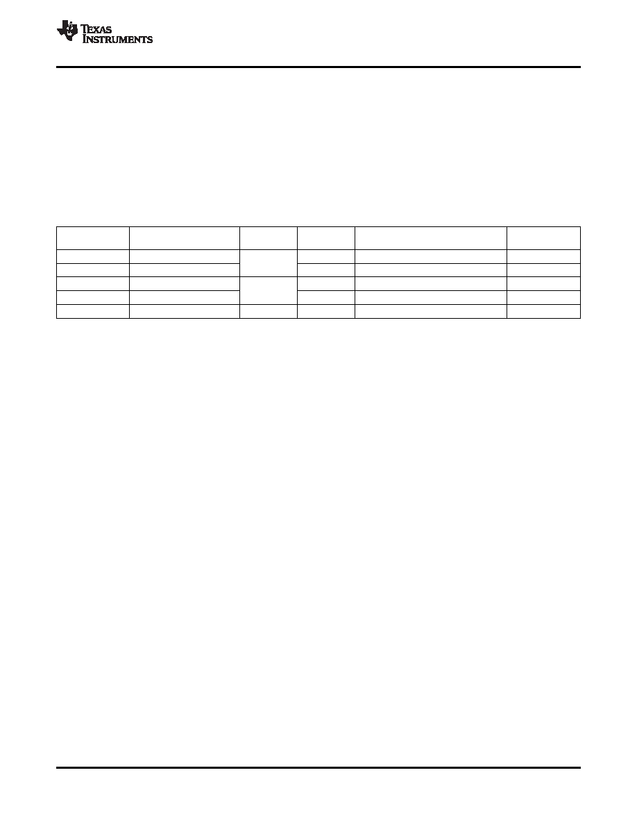
Table 3. Memory Selection Assignment
MEMORY
MEMORY SELECTED
MEMORY
MEMORY BASE ADDRESS
STATIC MEM
MPU
SELECT
(ALL INTERNAL)
SIZE
REGISTER
CTL REGISTER
0 (fine)
FLASH
NO
MFBAHR0 and MFBALR0
768K
1 (fine)
FLASH
NO
MFBAHR1 and MFBALR1
2 (fine)
RAM
YES
MFBAHR2 and MFBALR2
48K(1)
3 (fine)
RAM
YES
MFBAHR3 and MFBALR3
4 (fine)
HET RAM
1.5K
MFBAHR4 and MFBALR4
SMCR1
(1)
The starting addresses for both RAM memory-select signals cannot be offset from each other by a multiple of the user-defined block
size in the memory-base address register.
RAM
The B768 device contains 48K bytes of internal static RAM configurable by the SYS module to be addressed
within the range of 0x0000_0000 to 0xFFE0_0000. This B768 RAM is implemented in one 48K-byte array
selected by two memory-select signals. This B768 configuration imposes an additional constraint on the memory
map for RAM; the starting addresses for both RAM memory selects cannot be offset from each other by the
multiples of the size of the physical RAM (i.e., 48K bytes for the B768 device). The B768 RAM is addressed
through memory selects 2 and 3.
The RAM can be protected by the memory protection unit (MPU) portion of the SYS module, allowing the user
finer blocks of memory protection than is allowed by the memory selects. The MPU is ideal for protecting an
operating system while allowing access to the current task. For more detailed information on the MPU portion of
the SYS module and memory protection, see the memory section of the TMS470R1x System Module Reference
Guide (literature number SPNU189).
F05 Flash
The F05 flash memory is a nonvolatile electrically erasable and programmable memory implemented with a
32-bit-wide data bus interface. The F05 flash has an external state machine for program and erase functions.
See the flash read and flash program and erase sections below.
Flash Protection Keys
The
B768
device
provides
flash
protection
keys.
These
four
32-bit
protection
keys
prevent
program/erase/compaction operations from occurring until after the four protection keys have been matched by
the CPU loading the correct user keys into the FMPKEY control register. The protection keys on the B768 are
located in the last 4 words of the first 16K sector. For more detailed information on flash program and erase
operations, see the TMS470R1x F05 Flash Reference Guide (literature number SPNU213).
Flash Read
The B768 flash memory is configurable by the SYS module to be addressed within the range of 0x0000_0000 to
0xFFE0_0000. The flash is addressed through memory selects 0 and 1.
NOTE:
The flash external pump voltage (VCCP ) is required for all operations (program, erase,
and read).
Copyright 2005–2008, Texas Instruments Incorporated
13
Product Folder Link(s): TMS470R1B768
相关PDF资料 |
PDF描述 |
|---|---|
| TMS4C1050-4DJL | 256K X 4 OTHER FIFO, PDSO20 |
| TMS4C1050-3NL | 256K X 4 OTHER FIFO, PDIP16 |
| TMS570LS10216ASZWTQR | 32-BIT, FLASH, 160 MHz, RISC MICROCONTROLLER, PBGA337 |
| TMX320DM642GNZ500 | 64-BIT, 75.19 MHz, OTHER DSP, PBGA548 |
| TN4002PM | 10 MHz - 500 MHz RF/MICROWAVE WIDE BAND LOW POWER AMPLIFIER |
相关代理商/技术参数 |
参数描述 |
|---|---|
| TMS470R1B768PGET | 功能描述:ARM微控制器 - MCU 60mhz / 768k Flash RoHS:否 制造商:STMicroelectronics 核心:ARM Cortex M4F 处理器系列:STM32F373xx 数据总线宽度:32 bit 最大时钟频率:72 MHz 程序存储器大小:256 KB 数据 RAM 大小:32 KB 片上 ADC:Yes 工作电源电压:1.65 V to 3.6 V, 2 V to 3.6 V, 2.2 V to 3.6 V 工作温度范围:- 40 C to + 85 C 封装 / 箱体:LQFP-48 安装风格:SMD/SMT |
| TMS470R1F316PZQ | 制造商:Texas Instruments 功能描述: |
| TMS470R1F354PNQ | 制造商:Texas Instruments 功能描述: |
| TMS470R1F366APZQ | 制造商:Texas Instruments 功能描述: |
| TMS470R1F369APGEQ | 制造商:Texas Instruments 功能描述: |
发布紧急采购,3分钟左右您将得到回复。