- 您现在的位置:买卖IC网 > PDF目录98280 > TPS2540RTET (TEXAS INSTRUMENTS INC) 1-CHANNEL POWER SUPPLY SUPPORT CKT, PQCC16 PDF资料下载
参数资料
| 型号: | TPS2540RTET |
| 厂商: | TEXAS INSTRUMENTS INC |
| 元件分类: | 电源管理 |
| 英文描述: | 1-CHANNEL POWER SUPPLY SUPPORT CKT, PQCC16 |
| 封装: | GREEN, PLASTIC, WQFN-16 |
| 文件页数: | 23/37页 |
| 文件大小: | 999K |
| 代理商: | TPS2540RTET |
第1页第2页第3页第4页第5页第6页第7页第8页第9页第10页第11页第12页第13页第14页第15页第16页第17页第18页第19页第20页第21页第22页当前第23页第24页第25页第26页第27页第28页第29页第30页第31页第32页第33页第34页第35页第36页第37页
SLVSAG2A
– OCTOBER 2010 – REVISED APRIL 2011
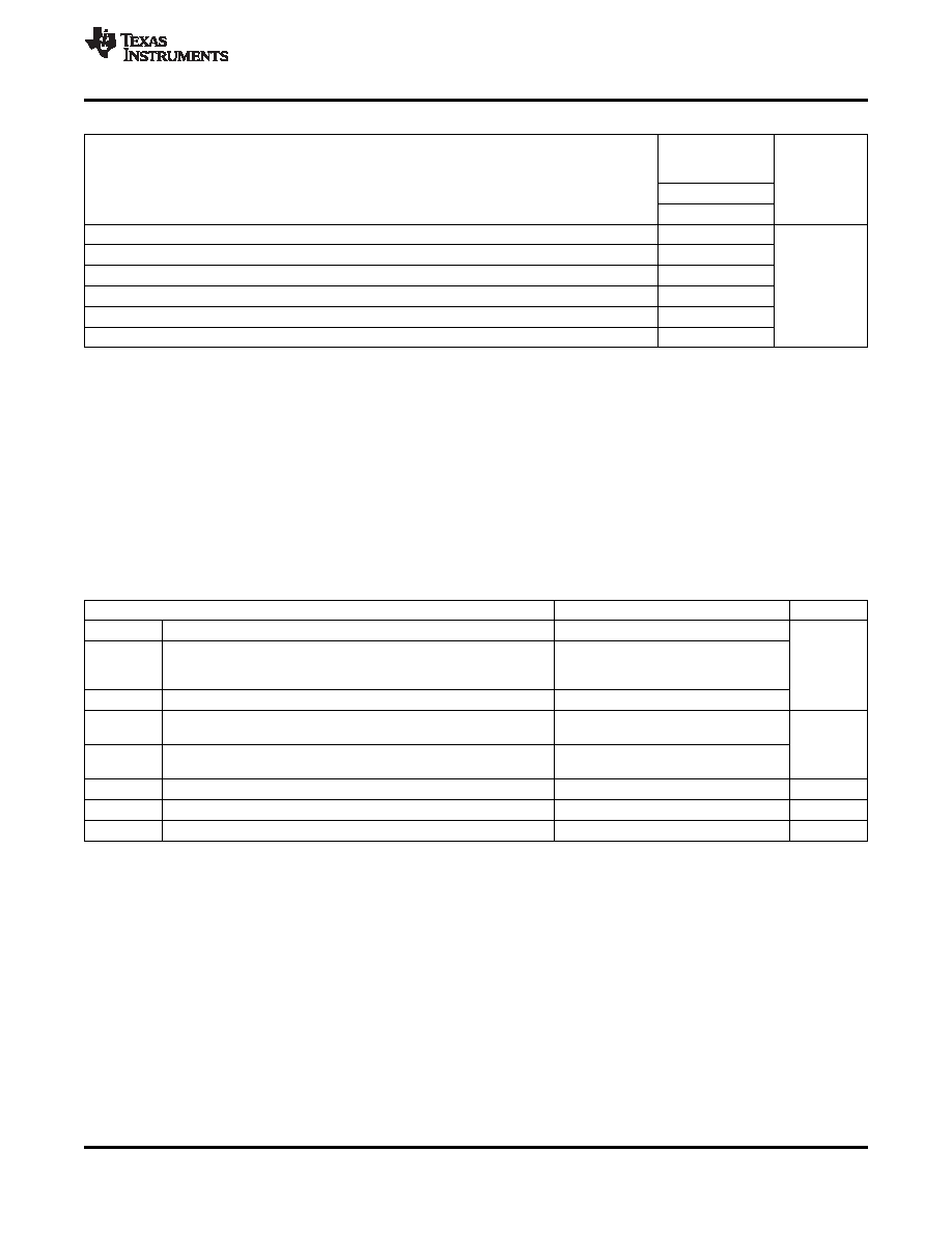
THERMAL INFORMATION
TPS2540
TPS2540A
TPS2541
THERMAL METRIC(1)
UNITS
RTE
16 PINS
θJA
Junction-to-ambient thermal resistance(2)
53.4
θJCtop
Junction-to-case (top) thermal resistance(3)
51.4
θJB
Junction-to-board thermal resistance(4)
17.2
°C/W
ψJT
Junction-to-top characterization parameter(5)
3.7
ψJB
Junction-to-board characterization parameter(6)
20.7
θJCbot
Junction-to-case (bottom) thermal resistance(7)
3.9
(1)
For more information about traditional and new thermal metrics, see the IC Package Thermal Metrics application report, SPRA953.
(2)
The junction-to-ambient thermal resistance under natural convection is obtained in a simulation on a JEDEC-standard, high-K board, as
specified in JESD51-7, in an environment described in JESD51-2a.
(3)
The junction-to-case (top) thermal resistance is obtained by simulating a cold plate test on the package top. No specific
JEDEC-standard test exists, but a close description can be found in the ANSI SEMI standard G30-88.
(4)
The junction-to-board thermal resistance is obtained by simulating in an environment with a ring cold plate fixture to control the PCB
temperature, as described in JESD51-8.
(5)
The junction-to-top characterization parameter,
ψJT, estimates the junction temperature of a device in a real system and is extracted
from the simulation data for obtaining
θJA, using a procedure described in JESD51-2a (sections 6 and 7).
(6)
The junction-to-board characterization parameter,
ψJB, estimates the junction temperature of a device in a real system and is extracted
from the simulation data for obtaining
θJA , using a procedure described in JESD51-2a (sections 6 and 7).
(7)
The junction-to-case (bottom) thermal resistance is obtained by simulating a cold plate test on the exposed (power) pad. No specific
JEDEC standard test exists, but a close description can be found in the ANSI SEMI standard G30-88.
RECOMMENDED OPERATING CONDITIONS
over operating free-air temperature range (unless otherwise noted)
PARAMETER
MIN
NOM
MAX
UNIT
VIN
Input voltage, IN
4.5
5.5
Input voltage, logic-level inputs,
(CTL1, CTL2, CTL3, EN (TPS2540/40A/41), DSC (TPS2541),
0
5.5
V
ILIM_SEL)
Input voltage, data line inputs, (DP_IN, DM_IN, DP_OUT, DM_OUT)
5.5
Continuous current, data line inputs,
±30
(SDP or CDP mode, DP_IN to DP_OUT or DM_IN to DM_OUT )
mA
Continuous current, data line inputs, (BC1.2 DCP mode, DP_IN to
±10
DM_IN)
IOUT
Continuous output current, OUT
0
2.5
A
RILIMx
Current-limit set resistors, (ILIM0 to GND, ILIM1 to GND)
16.9
750
k
Ω
TJ
Operating virtual junction temperature
-40
125
°C
Copyright
2010–2011, Texas Instruments Incorporated
3
相关PDF资料 |
PDF描述 |
|---|---|
| TPS2541RTET | 1-CHANNEL POWER SUPPLY SUPPORT CKT, PQCC16 |
| TPS2550DBV | 1-CHANNEL POWER SUPPLY SUPPORT CKT, PDSO6 |
| TPS2551DRVR | 1-CHANNEL POWER SUPPLY SUPPORT CKT, PDSO6 |
| TPS2551DRVTG4 | 1-CHANNEL POWER SUPPLY SUPPORT CKT, PDSO6 |
| TPS2551DRVRG4 | 1-CHANNEL POWER SUPPLY SUPPORT CKT, PDSO6 |
相关代理商/技术参数 |
参数描述 |
|---|---|
| TPS2540RTET | 制造商:Texas Instruments 功能描述:IC USB SWITCH 2.6GHZ 16-WQFN |
| TPS2541ARTER | 功能描述:电源开关 IC - USB USB Charging Port Pwr Sw & Controller RoHS:否 制造商:Micrel 电源电压-最小:2.7 V 电源电压-最大:5.5 V 最大工作温度:+ 85 C 最小工作温度:- 40 C 封装 / 箱体:SOIC-8 封装:Tube |
| TPS2541ARTET | 功能描述:电源开关 IC - USB USB Charging Port Pwr Sw & Controller RoHS:否 制造商:Micrel 电源电压-最小:2.7 V 电源电压-最大:5.5 V 最大工作温度:+ 85 C 最小工作温度:- 40 C 封装 / 箱体:SOIC-8 封装:Tube |
| TPS2541RTER | 功能描述:电源开关 IC - USB USB Charging Port Pwr Swtch &Contrller RoHS:否 制造商:Micrel 电源电压-最小:2.7 V 电源电压-最大:5.5 V 最大工作温度:+ 85 C 最小工作温度:- 40 C 封装 / 箱体:SOIC-8 封装:Tube |
| TPS2541RTET | 功能描述:电源开关 IC - USB USB Charging Port Pwr Swtch &Contrller RoHS:否 制造商:Micrel 电源电压-最小:2.7 V 电源电压-最大:5.5 V 最大工作温度:+ 85 C 最小工作温度:- 40 C 封装 / 箱体:SOIC-8 封装:Tube |
发布紧急采购,3分钟左右您将得到回复。