参数资料
| 型号: | TPS54260DRCR |
| 厂商: | Texas Instruments |
| 文件页数: | 14/52页 |
| 文件大小: | 0K |
| 描述: | IC REG BUCK ADJ 2.5A 10SON |
| 标准包装: | 3,000 |
| 系列: | SWIFT™, Eco-Mode™ |
| 类型: | 降压(降压) |
| 输出类型: | 可调式 |
| 输出数: | 1 |
| 输出电压: | 0.8 V ~ 58 V |
| 输入电压: | 3.5 V ~ 60 V |
| PWM 型: | 电流模式 |
| 频率 - 开关: | 100kHz ~ 2.5MHz |
| 电流 - 输出: | 2.5A |
| 同步整流器: | 无 |
| 工作温度: | -40°C ~ 150°C |
| 安装类型: | 表面贴装 |
| 封装/外壳: | 10-VFDFN 裸露焊盘 |
| 包装: | 带卷 (TR) |
| 供应商设备封装: | 10-SON 裸露焊盘(3x3) |
第1页第2页第3页第4页第5页第6页第7页第8页第9页第10页第11页第12页第13页当前第14页第15页第16页第17页第18页第19页第20页第21页第22页第23页第24页第25页第26页第27页第28页第29页第30页第31页第32页第33页第34页第35页第36页第37页第38页第39页第40页第41页第42页第43页第44页第45页第46页第47页第48页第49页第50页第51页第52页
�� ��
��
��SLVSA86A� –� MARCH� 2010� –� REVISED� DECEMBER� 2010�
�www.ti.com�
�DETAILED� DESCRIPTION� (continued)�
�Adjusting� the� Output� Voltage�
�The� output� voltage� is� set� with� a� resistor� divider� from� the� output� node� to� the� VSENSE� pin.� It� is� recommended� to�
�use� 1%� tolerance� or� better� divider� resistors.� Start� with� a� 10� k� ?� for� the� R2� resistor� and� use� the� Equation� 1� to�
�calculate� R1.� To� improve� efficiency� at� light� loads� consider� using� larger� value� resistors.� If� the� values� are� too� high�
�the� regulator� will� be� more� susceptible� to� noise� and� voltage� errors� from� the� VSENSE� input� current� will� be�
�noticeable.�
�è� ?�
�? Vout - 0.8V ?�
�R1� =� R2� ′� ?� ÷�
�0.8� V�
�(1)�
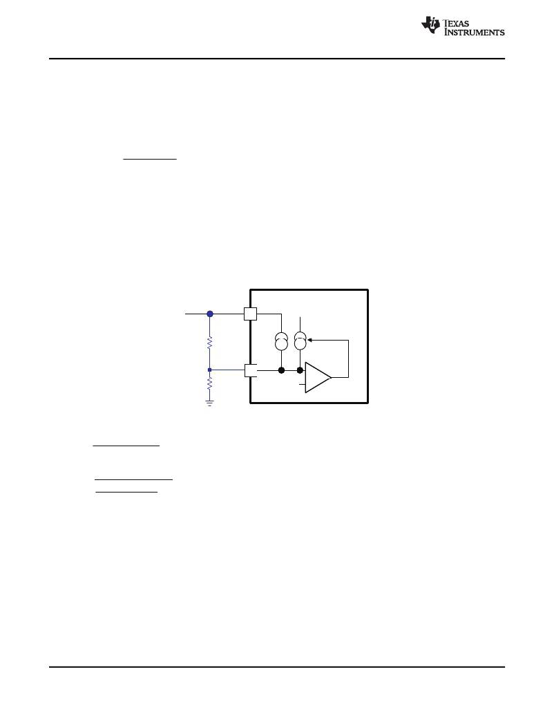
�Enable� and� Adjusting� Undervoltage� Lockout�
�The� TPS54260� is� disabled� when� the� VIN� pin� voltage� falls� below� 2.5� V.� If� an� application� requires� a� higher�
�undervoltage� lockout� (UVLO),� use� the� EN� pin� as� shown� in� Figure� 27� to� adjust� the� input� voltage� UVLO� by� using�
�the� two� external� resistors.� Though� it� is� not� necessary� to� use� the� UVLO� adjust� registers,� for� operation� it� is� highly�
�recommended� to� provide� consistent� power� up� behavior.� The� EN� pin� has� an� internal� pull-up� current� source,� I1,� of�
�0.9� m� A� that� provides� the� default� condition� of� the� TPS54260� operating� when� the� EN� pin� floats.� Once� the� EN� pin�
�voltage� exceeds� 1.25V,� an� additional� 2.9� m� A� of� hysteresis,� Ihys,� is� added.� This� additional� current� facilitates� input�
�voltage� hysteresis.� Use� Equation� 2� to� set� the� external� hysteresis� for� the� input� voltage.� Use� Equation� 3� to� set� the�
�input� start� voltage.�
�TPS54260�
�VIN�
�R1�
�I1�
�0.9� m� A�
�+�
�Ihys�
�2.9� m� A�
�R2�
�EN�
�1.25� V�
�-�
�Figure� 27.� Adjustable� Undervoltage� Lockout� (UVLO)�
�-� V�
�R1� =� START� STOP�
�V�
�I� HYS�
�(2)�
�R2� =�
�V� ENA�
�V� START� -� V� ENA�
�R1�
�+� I� 1�
�(3)�
�Another� technique� to� add� input� voltage� hysteresis� is� shown� in� Figure� 28� .� This� method� may� be� used,� if� the�
�resistance� values� are� high� from� the� previous� method� and� a� wider� voltage� hysteresis� is� needed.� The� resistor� R3�
�sources� additional� hysteresis� current� into� the� EN� pin.�
�14�
��Product� Folder� Link(s):� TPS54260�
�Copyright� ?� 2010,� Texas� Instruments� Incorporated�
�相关PDF资料 |
PDF描述 |
|---|---|
| TPS54326RGTT | IC REG BUCK SYNC ADJ 3A 16QFN |
| TPS54478RTER | IC REG BUCK SYNC ADJ 4A 16WQFN |
| TPS54550PWPG4 | IC REG BUCK SYNC ADJ 6A 16HTSSOP |
| TPS54678RTER | IC REG BUCK SYNC ADJ 6A 16WQFN |
| TPS54900PWRG4 | IC REG BUCK ADJ .1A QUAD 16TSSOP |
相关代理商/技术参数 |
参数描述 |
|---|---|
| TPS54260DRCT | 功能描述:直流/直流开关转换器 3.5V-60Vin,2.5A,2.5 MHz Step Down SWIFT RoHS:否 制造商:STMicroelectronics 最大输入电压:4.5 V 开关频率:1.5 MHz 输出电压:4.6 V 输出电流:250 mA 输出端数量:2 最大工作温度:+ 85 C 安装风格:SMD/SMT |
| TPS54260EVM-597 | 功能描述:电源管理IC开发工具 2.5A,10.8-13.2Vin SWIFT Conv Eval Mod RoHS:否 制造商:Maxim Integrated 产品:Evaluation Kits 类型:Battery Management 工具用于评估:MAX17710GB 输入电压: 输出电压:1.8 V |
| TPS54260MDGQTEP | 功能描述:IC REG BUCK ADJ 2.5A 10MOSP 制造商:texas instruments 系列:Eco-Mode? 包装:剪切带(CT) 零件状态:在售 功能:降压 输出配置:正 拓扑:降压 输出类型:可调式 输出数:1 电压 - 输入(最小值):3.5V 电压 - 输入(最大值):60V 电压 - 输出(最小值/固定):0.8V 电压 - 输出(最大值):60V 电流 - 输出:2.5A 频率 - 开关:100kHz ~ 2.5MHz 同步整流器:无 工作温度:-40°C ~ 150°C(TJ) 安装类型:表面贴装 封装/外壳:10-TFSOP,10-MSOP(0.118",3.00mm 宽)裸露焊盘 供应商器件封装:10-MSOP-PowerPad 标准包装:1 |
| TPS54260MDRCTEP | 功能描述:IC REG BUCK ADJ 2.5A 10VSON 制造商:texas instruments 系列:Eco-Mode? 包装:剪切带(CT) 零件状态:在售 功能:降压 输出配置:正 拓扑:降压 输出类型:可调式 输出数:1 电压 - 输入(最小值):3.5V 电压 - 输入(最大值):60V 电压 - 输出(最小值/固定):0.8V 电压 - 输出(最大值):60V 电流 - 输出:2.5A 频率 - 开关:100kHz ~ 2.5MHz 同步整流器:无 工作温度:-40°C ~ 150°C(TJ) 安装类型:表面贴装 封装/外壳:10-VFDFN 裸露焊盘 供应商器件封装:10-VSON(3x3) 标准包装:1 |
| TPS54260-Q1 | 制造商:TI 制造商全称:Texas Instruments 功能描述:3.5 V to 60 V STEP DOWN CONVERTER WITH ECO-MODEa?¢ |
发布紧急采购,3分钟左右您将得到回复。