参数资料
| 型号: | TPS54260DRCR |
| 厂商: | Texas Instruments |
| 文件页数: | 38/52页 |
| 文件大小: | 0K |
| 描述: | IC REG BUCK ADJ 2.5A 10SON |
| 标准包装: | 3,000 |
| 系列: | SWIFT™, Eco-Mode™ |
| 类型: | 降压(降压) |
| 输出类型: | 可调式 |
| 输出数: | 1 |
| 输出电压: | 0.8 V ~ 58 V |
| 输入电压: | 3.5 V ~ 60 V |
| PWM 型: | 电流模式 |
| 频率 - 开关: | 100kHz ~ 2.5MHz |
| 电流 - 输出: | 2.5A |
| 同步整流器: | 无 |
| 工作温度: | -40°C ~ 150°C |
| 安装类型: | 表面贴装 |
| 封装/外壳: | 10-VFDFN 裸露焊盘 |
| 包装: | 带卷 (TR) |
| 供应商设备封装: | 10-SON 裸露焊盘(3x3) |
第1页第2页第3页第4页第5页第6页第7页第8页第9页第10页第11页第12页第13页第14页第15页第16页第17页第18页第19页第20页第21页第22页第23页第24页第25页第26页第27页第28页第29页第30页第31页第32页第33页第34页第35页第36页第37页当前第38页第39页第40页第41页第42页第43页第44页第45页第46页第47页第48页第49页第50页第51页第52页
�� ��
��
��SLVSA86A� –� MARCH� 2010� –� REVISED� DECEMBER� 2010�
�www.ti.com�
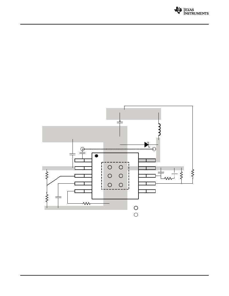
�Layout�
�Layout� is� a� critical� portion� of� good� power� supply� design.� There� are� several� signals� paths� that� conduct� fast�
�changing� currents� or� voltages� that� can� interact� with� stray� inductance� or� parasitic� capacitance� to� generate� noise�
�or� degrade� the� power� supplies� performance.� To� help� eliminate� these� problems,� the� VIN� pin� should� be� bypassed�
�to� ground� with� a� low� ESR� ceramic� bypass� capacitor� with� X5R� or� X7R� dielectric.� Care� should� be� taken� to�
�minimize� the� loop� area� formed� by� the� bypass� capacitor� connections,� the� VIN� pin,� and� the� anode� of� the� catch�
�diode.� See� Figure� 62� for� a� PCB� layout� example.� The� GND� pin� should� be� tied� directly� to� the� power� pad� under� the�
�IC� and� the� power� pad.�
�The� power� pad� should� be� connected� to� any� internal� PCB� ground� planes� using� multiple� vias� directly� under� the� IC.�
�The� PH� pin� should� be� routed� to� the� cathode� of� the� catch� diode� and� to� the� output� inductor.� Since� the� PH�
�connection� is� the� switching� node,� the� catch� diode� and� output� inductor� should� be� located� close� to� the� PH� pins,�
�and� the� area� of� the� PCB� conductor� minimized� to� prevent� excessive� capacitive� coupling.� For� operation� at� full� rated�
�load,� the� top� side� ground� area� must� provide� adequate� heat� dissipating� area.� The� RT/CLK� pin� is� sensitive� to� noise�
�so� the� RT� resistor� should� be� located� as� close� as� possible� to� the� IC� and� routed� with� minimal� lengths� of� trace.� The�
�additional� external� components� can� be� placed� approximately� as� shown.� It� may� be� possible� to� obtain� acceptable�
�performance� with� alternate� PCB� layouts,� however� this� layout� has� been� shown� to� produce� good� results� and� is�
�meant� as� a� guideline.�
�Vout�
�Output�
�Topside�
�Capacitor�
�Output�
�Inductor�
�Ground�
�Area�
�Route� Boot� Capacitor�
�Trace� on� another� layer� to�
�provide� wide� path� for�
�Catch�
�Diode�
�topside� ground�
�Input�
�Bypass�
�Vin�
�Capacitor�
�BOOT�
�VIN�
�EN�
�PH�
�GND�
�COMP�
�UVLO�
�Adjust�
�Resistors�
�Slow� Start�
�Capacitor�
�SS/TR�
�RT/CLK�
�Frequency�
�Set� Resistor�
�VSENSE�
�PWRGD�
�Thermal� VIA�
�Compensation�
�Network�
�Resistor�
�Divider�
�Signal� VIA�
�Figure� 62.� PCB� Layout� Example�
�Estimated� Circuit� Area�
�The� estimated� printed� circuit� board� area� for� the� components� used� in� the� design� of� Figure� 49� is� 0.55� in� 2� .� This� area�
�does� not� include� test� points� or� connectors.�
�38�
��Product� Folder� Link(s):� TPS54260�
�Copyright� ?� 2010,� Texas� Instruments� Incorporated�
�相关PDF资料 |
PDF描述 |
|---|---|
| TPS54326RGTT | IC REG BUCK SYNC ADJ 3A 16QFN |
| TPS54478RTER | IC REG BUCK SYNC ADJ 4A 16WQFN |
| TPS54550PWPG4 | IC REG BUCK SYNC ADJ 6A 16HTSSOP |
| TPS54678RTER | IC REG BUCK SYNC ADJ 6A 16WQFN |
| TPS54900PWRG4 | IC REG BUCK ADJ .1A QUAD 16TSSOP |
相关代理商/技术参数 |
参数描述 |
|---|---|
| TPS54260DRCT | 功能描述:直流/直流开关转换器 3.5V-60Vin,2.5A,2.5 MHz Step Down SWIFT RoHS:否 制造商:STMicroelectronics 最大输入电压:4.5 V 开关频率:1.5 MHz 输出电压:4.6 V 输出电流:250 mA 输出端数量:2 最大工作温度:+ 85 C 安装风格:SMD/SMT |
| TPS54260EVM-597 | 功能描述:电源管理IC开发工具 2.5A,10.8-13.2Vin SWIFT Conv Eval Mod RoHS:否 制造商:Maxim Integrated 产品:Evaluation Kits 类型:Battery Management 工具用于评估:MAX17710GB 输入电压: 输出电压:1.8 V |
| TPS54260MDGQTEP | 功能描述:IC REG BUCK ADJ 2.5A 10MOSP 制造商:texas instruments 系列:Eco-Mode? 包装:剪切带(CT) 零件状态:在售 功能:降压 输出配置:正 拓扑:降压 输出类型:可调式 输出数:1 电压 - 输入(最小值):3.5V 电压 - 输入(最大值):60V 电压 - 输出(最小值/固定):0.8V 电压 - 输出(最大值):60V 电流 - 输出:2.5A 频率 - 开关:100kHz ~ 2.5MHz 同步整流器:无 工作温度:-40°C ~ 150°C(TJ) 安装类型:表面贴装 封装/外壳:10-TFSOP,10-MSOP(0.118",3.00mm 宽)裸露焊盘 供应商器件封装:10-MSOP-PowerPad 标准包装:1 |
| TPS54260MDRCTEP | 功能描述:IC REG BUCK ADJ 2.5A 10VSON 制造商:texas instruments 系列:Eco-Mode? 包装:剪切带(CT) 零件状态:在售 功能:降压 输出配置:正 拓扑:降压 输出类型:可调式 输出数:1 电压 - 输入(最小值):3.5V 电压 - 输入(最大值):60V 电压 - 输出(最小值/固定):0.8V 电压 - 输出(最大值):60V 电流 - 输出:2.5A 频率 - 开关:100kHz ~ 2.5MHz 同步整流器:无 工作温度:-40°C ~ 150°C(TJ) 安装类型:表面贴装 封装/外壳:10-VFDFN 裸露焊盘 供应商器件封装:10-VSON(3x3) 标准包装:1 |
| TPS54260-Q1 | 制造商:TI 制造商全称:Texas Instruments 功能描述:3.5 V to 60 V STEP DOWN CONVERTER WITH ECO-MODEa?¢ |
发布紧急采购,3分钟左右您将得到回复。