- 您现在的位置:买卖IC网 > PDF目录365968 > TSB14AA1 FPGA (Field-Programmable Gate Array) PDF资料下载
参数资料
| 型号: | TSB14AA1 |
| 英文描述: | FPGA (Field-Programmable Gate Array) |
| 中文描述: | 电机及电子学工程师联合会1394-1995。 3.3。 1-port.50/100Mbps。底板PHY |
| 文件页数: | 9/35页 |
| 文件大小: | 224K |
| 代理商: | TSB14AA1 |
第1页第2页第3页第4页第5页第6页第7页第8页当前第9页第10页第11页第12页第13页第14页第15页第16页第17页第18页第19页第20页第21页第22页第23页第24页第25页第26页第27页第28页第29页第30页第31页第32页第33页第34页第35页
1
–
4
1.5
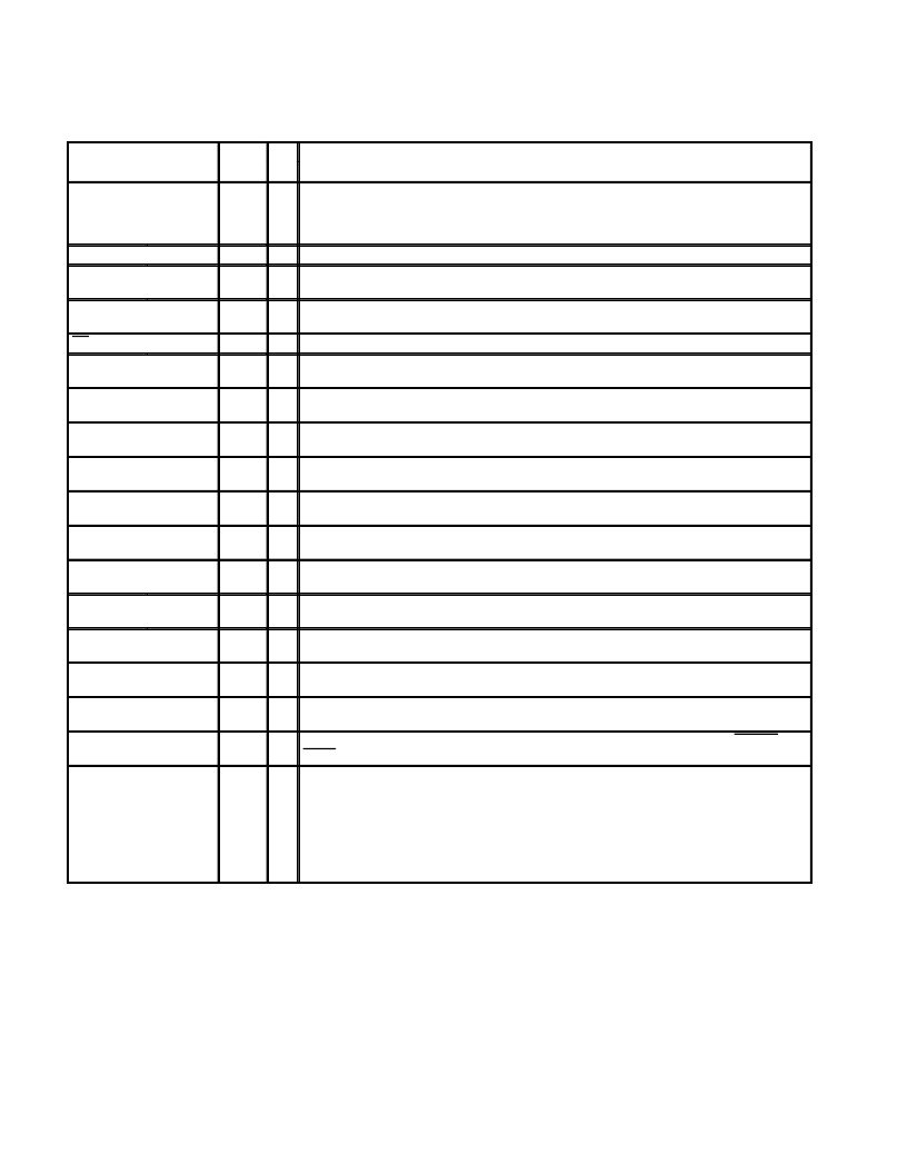
Terminal Descriptions
TERMINAL
TYPE
I/O
DESCRIPTION
NAME
CLK_SEL0
NO.
46
CMOS
I
Clock select 0. If this terminal is set to low (0) then the speed is 98.304 Mbps. If this terminal is set to
high (1) the speed is 49.152 Mbps.
To operate at 100 Mbps requires an input clock of 98.304 MHz. To operate at 49.152 Mbps requires
an input clock of 49.152 MHz.
Clock select 1. CLK_SEL1 must be tied to ground during normal operation.
CLK_SEL1
47
CMOS
I
CTL0, CTL1
7, 8
CMOS
I/O
Control I/O. These are bidirectional signals that communicate between the TSB14AA1A and the
link layer that controls the passage of information between the two devices.
Data I/O. These are bidirectional information signals that communicate the data between the
TSB14AA1A and the link layer controller.
Enable on-chip regulator. This active low pin enables the 1.8 V on
–
chip regulator.
D0, D1
10, 12
CMOS
I/O
EN
38
Supply
I
EX_ID0
19
CMOS
I
External ID 0. The state of this pin sets the value of bit 0 of the
PHYSICAL_ID
field in the
NODE ID
Register upon hardware or SWHRST reset. The register bit may be modified by software.
External ID 1. The state of this pin sets the value of bit 1 of the
PHYSICAL_ID
field in the
NODE ID
register upon hardware or SWHRST reset. The register bit may be modified by software.
External ID 2. The state of this pin sets the value of bit 2 of the
PHYSICAL_ID
field in the
NODE ID
register upon hardware or SWHRST reset. The register bit may be modified by software.
External ID 3. The state of this pin sets the value of bit 3 of the
PHYSICAL_ID
field in the
NODE ID
register upon hardware or SWHRST reset. The register bit may be modified by software.
External ID 4. The state of this pin sets the value of bit 4 of the
PHYSICAL_ID
field in the
NODE ID
register upon hardware or SWHRST reset. The register bit may be modified by software.
External ID 5. The state of this pin sets the value of bit 5 of the
PHYSICAL_ID
field in the
NODE ID
register upon hardware or SWHRST reset. The register bit may be modified by software.
External priority 0. The state of this pin sets the value of bit 0 of the
PRIORITY
field in the
PRIORITY
register upon hardware or SWHRST reset. The register bit may be modified by software.
External priority 1. The state of this pin sets the value of bit 1 of the
PRIORITY
field in the
PRIORITY
register upon hardware or SWHRST reset. The register bit may be modified by software.
External priority 2. The state of this pin sets the value of bit 2 of the
PRIORITY
field in the
PRIORITY
register upon hardware or SWHRST reset. The register bit may be modified by software.
External priority 3. The state of this pin sets the value of bit 3 of the
PRIORITY
field in the
PRIORITY
register upon hardware or SWHRST reset. The register bit may be modified by software.
Ground voltage reference
EX_ID1
20
CMOS
I
EX_ID2
21
CMOS
I
EX_ID3
22
CMOS
I
EX_ID4
23
CMOS
I
EX_ID5
24
CMOS
I
EX_PR0
13
CMOS
I
EX_PR1
14
CMOS
I
EX_PR2
15
CMOS
I
EX_PR3
16
CMOS
I
GND
4, 18, 28,
32, 34, 44
9
Supply
IDS
CMOS
I
Invert data strobe. When this pin is set low, the TDATA, TSTRB, RDATA, RSTRB, OCDOE, and
TDOE pins operate normally (i.e., true). When this pin is set high, these six pins are inverted.
Link-On output. This pin notifies the LLC to power-up and become active. LINKON is a square-wave
signal with a frequency between 4 and 8 MHz when active. LINKON is otherwise driven low, except
during a hardware reset when it is high impedance.
LINKON is activated if the LPS is inactive (LLC inactive) and when the PHY receives a link-on PHY
packet addressed to this node.
Once activated, LINKON will continue active until the LPS becomes active (LLC active). The PHY
also deasserts (low) LINKON when a bus-reset occurs.
LINKON
2
CMOS
O
相关PDF资料 |
PDF描述 |
|---|---|
| TSB14AA1I | FPGA (Field-Programmable Gate Array) |
| TSB14AA1T | FPGA (Field-Programmable Gate Array) |
| TSB14C01MHV | IC APEX 20KE FPGA 160K 484-FBGA |
| TSB14C01HV | 5-V IEEE 1394-1995 BACKPLANE TRANSCEIVER/ARBITER |
| TSB21LV03MHV | IC APEX 20KE FPGA 200K 484-FBGA |
相关代理商/技术参数 |
参数描述 |
|---|---|
| TSB14AA1A | 制造商:TI 制造商全称:Texas Instruments 功能描述:3.3 V IEEE 1394-1995 BACKPLANE PHY |
| TSB14AA1AI | 制造商:TI 制造商全称:Texas Instruments 功能描述:3.3 V IEEE 1394-1995 BACKPLANE PHY |
| TSB14AA1AIPFB | 功能描述:1394 接口集成电路 IEEE139419953.3V1prt 50/100Mbps BkplnPHY RoHS:否 制造商:Texas Instruments 类型:Link Layer Controller 工作电源电压: 封装 / 箱体:LQFP 封装:Tray |
| TSB14AA1AIPFBG4 | 功能描述:1394 接口集成电路 3.3V 1-port 50/100 Mbps Backplane PHY RoHS:否 制造商:Texas Instruments 类型:Link Layer Controller 工作电源电压: 封装 / 箱体:LQFP 封装:Tray |
| TSB14AA1APFB | 功能描述:1394 接口集成电路 3.3V 1-port 50/100 Mbps Backplane PHY RoHS:否 制造商:Texas Instruments 类型:Link Layer Controller 工作电源电压: 封装 / 箱体:LQFP 封装:Tray |
发布紧急采购,3分钟左右您将得到回复。