- 您现在的位置:买卖IC网 > Datasheet目录529 > UPA679TB-T2-A (Renesas Electronics America)MOSFET N/P-CH 20V SC-70 Datasheet资料下载
参数资料
| 型号: | UPA679TB-T2-A |
| 厂商: | Renesas Electronics America |
| 文件页数: | 3/12页 |
| 文件大小: | 0K |
| 描述: | MOSFET N/P-CH 20V SC-70 |
| 标准包装: | 3,000 |
| FET 型: | N 和 P 沟道 |
| FET 特点: | 逻辑电平门 |
| 漏极至源极电压(Vdss): | 20V |
| 电流 - 连续漏极(Id) @ 25° C: | 350mA,250mA |
| 开态Rds(最大)@ Id, Vgs @ 25° C: | 570 毫欧 @ 300mA,4.5V |
| 输入电容 (Ciss) @ Vds: | 28pF @ 10V |
| 功率 - 最大: | 200mW |
| 安装类型: | 表面贴装 |
| 封装/外壳: | 6-TSSOP,SC-88,SOT-363 |
| 供应商设备封装: | SC-88 |
| 包装: | 带卷 (TR) |
�� ��
��
��DATA� SHEET�
�MOS� FIELD� EFFECT� TRANSISTOR�
�μ� PA679TB�
�N/P-CHANNEL� MOS� FIELD� EFFECT� TRANSISTOR�
�FOR� SWITCHING�
�DESCRIPTION�
�The� μ� PA679TB� is� a� switching� device,� which� can� be� driven� directly� by� a� 2.5� V� power� source.�
�The� μ� PA679TB� features� a� low� on-state� resistance� and� excellent� switching� characteristics,� and� is� suitable� for�
�applications� such� as� power� switch� of� portable� machine� and� so� on.�
�FEATURES�
�?� 2.5� V� drive� available�
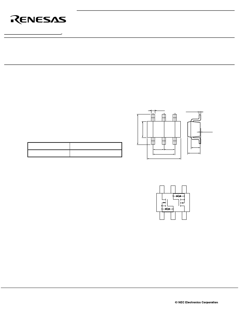
�PACKAGE� DRAWING� (Unit:� mm)�
�0.2� -� 0�
�0.15� -� 0.05�
�?� Low� on-state� resistance�
�N-ch� R� DS(on)1� =� 0.57� ?� MAX.� (V� GS� =� 4.5� V,� I� D� =� 0.30� A)�
�R� DS(on)3� =� 0.88� ?� MAX.� (V� GS� =� 2.5� V,� I� D� =� 0.15� A)�
�+0.1�
�+0.1�
�P-ch� R� DS(on)1� =� 1.45� ?� MAX.� (V� GS� =� ?� 4.5� V,� I� D� =� ?� 0.20� A)�
�R� DS(on)3� =� 2.98� ?� MAX.� (V� GS� =� ?� 2.5� V,� I� D� =� ?� 0.15� A)�
�?� Two� MOS� FET� circuits� in� same� size� package� as� SC-70�
�ORDERING� INFORMATION�
�6�
�1�
�5�
�2�
�4�
�3�
�0� to� 0.1�
�PART� NUMBER�
�PACKAGE�
�0.65�
�0.65�
�0.7�
�μ� PA679TB�
�Marking:� YA�
�SC-88� (SSP)�
�1.3�
�2.0� ±0.2�
�0.9 ±0.1�
�ABSOLUTE� MAXIMUM� RATINGS� (T� A� =� 25°C)�
�Drain� to� Source� Voltage� (V� GS� =� 0� V)� V� DSS�
�20� /� ?� 20�
�V�
�PIN� CONNECTION� (Top� View)�
�Gate� to� Source� Voltage� (V� DS� =� 0� V)�
�Drain� Current� (DC)�
�Note1�
�Drain� Current� (pulse)�
�V� GSS�
�I� D(DC)�
�I� D(pulse)�
�±� 12� /� m� 12�
�±� 0.35� /� m� 0.25�
�±� 1.40� /� m� 1.00�
�V�
�A�
�A�
�6�
�5�
�4�
�Total� Power� Dissipation� (2� units)�
�Channel� Temperature�
�Storage� Temperature�
�Note2�
�P� T�
�T� ch�
�T� stg�
�0.2�
�150�
�–55� to� +150�
�W�
�°C�
�°C�
�1.�
�2.�
�3.�
�4.�
�5.�
�Source� 1�
�Gate� 1�
�Drain� 2�
�Source� 2�
�Gate� 2�
�2.� Mounted� on� FR-4� board� of� 2500� mm� x� 1.1� mm�
�Notes� 1.� PW� ≤� 10� μ� s,� Duty� Cycle� ≤� 1%�
�2�
�1�
�2�
�3�
�6.�
�Drain� 1�
�Remark� The� diode� connected� between� the� gate� and� source� of� the� transistor� serves� as� a� protector� against� ESD.�
�When� this� device� actually� used,� an� additional� protection� circuit� is� externally� required� if� a� voltage� exceeding�
�the� rated� voltage� may� be� applied� to� this� device.�
�Caution� This� product� is� electrostatic-sensitive� device� due� to� low� ESD� capability� and� shoud� be� handled� with�
�caution� for� electrostatic� discharge.�
�V� ESD� =� ±� 100� V� TYP.� (C� =� 200� pF,� R� =� 0� ?� ,� Single� pulse)�
�The� information� in� this� document� is� subject� to� change� without� notice.� Before� using� this� document,� please�
�confirm� that� this� is� the� latest� version.�
�Not� all� products� and/or� types� are� available� in� every� country.� Please� check� with� an� NEC� Electronics�
�sales� representative� for� availability� and� additional� information.�
�Document� No.� G16615EJ1V0DS00� (1st� edition)�
�Date� Published� February� 2003� NS� CP(K)�
�Printed� in� Japan�
�2003�
�相关PDF资料 |
PDF描述 |
|---|---|
| UPB1007K-E1-A | IC DOWNCONVERT DL 3V 36-QFN |
| UPB1008K-EVAL | EVAL BOARD FOR UPB1008K |
| UPB1009K-E1-A | IC GPS RECEIVER LP 44-QFN |
| UPB1507GV-E1-A | MMIC PRESCALER 3GHZ 8-SSOP |
| UPB1508GV-E1 | MMIC PRESCALER 3GHZ 8-SSOP |
相关代理商/技术参数 |
参数描述 |
|---|---|
| UPA67C | 制造商:NEC 制造商全称:NEC 功能描述:微型打印机驱动程序的NPN硅外延达林顿晶体管阵列 |
| UPA75HA | 制造商:Panasonic Industrial Company 功能描述:TRANSISTOR |
| UPA80 | 制造商:未知厂家 制造商全称:未知厂家 功能描述:UPA80C Data Sheet | Data Sheet[02/1982] |
| UPA800T | 制造商:NEC 制造商全称:NEC 功能描述:HIGH-FREQUENCY LOW NOISE AMPLIFIER NPN SILICON EPITAXIAL TRANSISTOR WITH BUILT-IN 2 ELEMENTS MINI MOLD |
| UPA800T-A | 功能描述:射频双极小信号晶体管 NPN Silicn AMP Oscilltr Twn Trnst RoHS:否 制造商:NXP Semiconductors 配置:Single 晶体管极性:NPN 最大工作频率:7000 MHz 集电极—发射极最大电压 VCEO:15 V 发射极 - 基极电压 VEBO:2 V 集电极连续电流:0.15 A 功率耗散:1000 mW 直流集电极/Base Gain hfe Min: 最大工作温度:+ 150 C 封装 / 箱体:SOT-223 封装:Reel |
发布紧急采购,3分钟左右您将得到回复。