- 您现在的位置:买卖IC网 > PDF目录297646 > UT65L168(I) Pseudo Low Power SRAM PDF资料下载
参数资料
| 型号: | UT65L168(I) |
| 英文描述: | Pseudo Low Power SRAM |
| 中文描述: | 伪低功率SRAM |
| 文件页数: | 9/13页 |
| 文件大小: | 175K |
| 代理商: | UT65L168(I) |
UTRON
UT65L1616(E)/UT65L1616(I)
Rev. 1.1
1M X 16 BITS LOW POWER PSEUDO SRAM
UTRON TECHNOLOGY INC.
P80080
1F, No. 11, R&D Rd. II, Science-Based Industrial Park, Hsinchu, Taiwan, R. O. C.
TEL: 886-3-5777882
FAX: 886-3-5777919
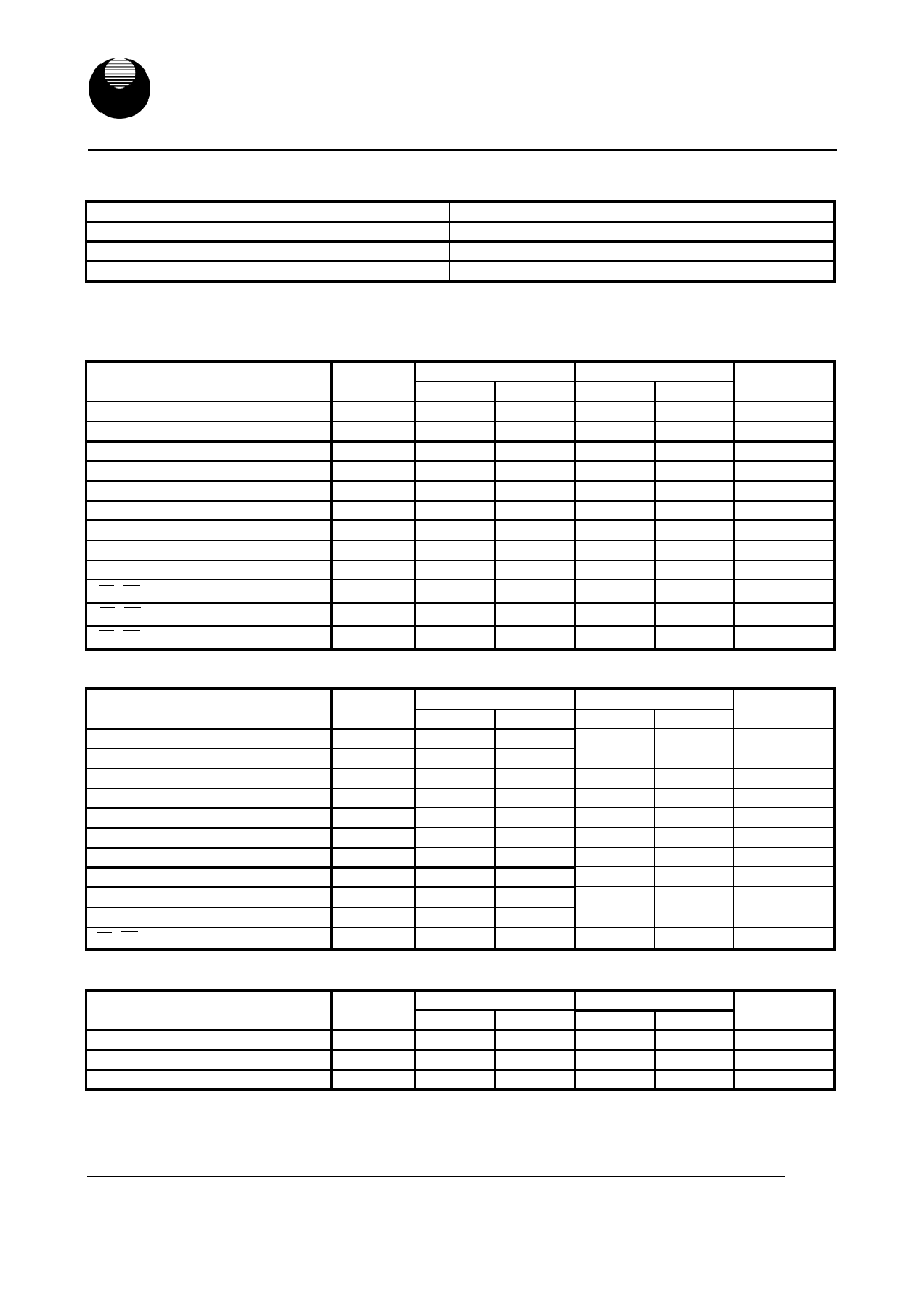
5
AC TEST CONDITIONS
Input Pulse Levels
0.2V to 2.4V
Input Rise and Fall Times
5ns
Input and Output Timing Reference Levels
1.5V
Output Load
CL = 30pF+1TTL, IOH/IOL = -1mA / 2mA
AC ELECTRICAL CHARACTERISTICS (VCC =2.5V~3.3V)
(1) READ CYCLE
UT65L1616-60
UT65L1616-70
PARAMETER
SYMBOL
MIN.
MAX.
MIN.
MAX.
UNIT
Read Cycle Time
tRC
60
40k
70
40k
ns
Address Access Time
tAA
-
60
-
70
ns
Chip enable to output
tACE
-
60
-
70
ns
Output Enable to Valid Output
tOE
-
25
-
25
ns
Chip enable to Low-Z output
tCLZ
10
-
10
-
ns
Output Enable to Low-Z Output
tOLZ
5
-
5
-
ns
Chip Disable to High-Z Output
tCHZ
0
5
0
5
ns
Output Disable to High-Z Output
tOHZ
0
5
0
5
ns
Output Hold from Address Change
tOH
5
-
5
-
ns
LB , UB Access Time
tBA
-
60
-
70
ns
LB , UB Disable to High-Z Output
tBHZ
0
5
0
5
ns
LB , UB Enable to Low-Z Output
tBLZ
10
-
10
-
ns
(2) WRITE CYCLE
UT65L1616-60
UT65L1616-70
PARAMETER
SYMBOL
MIN.
MAX.
MIN.
MAX.
UNIT
Write Cycle Time
tWC
60
40k
70
40k
ns
Address Valid to End of Write
tAW
50
-
60
-
ns
Chip enable to End of Write
tCW
50
-
60
-
ns
Address Set-up Time
tAS
0
-
0
-
ns
Write Pulse Width
tWP
50
-
50
-
ns
Write Recovery Time
tWR
0
-
0
-
ns
Data to Write Time Overlap
tDW
20
-
20
-
ns
Data Hold from Write Time
tDH
0
-
0
-
ns
End Write to Output Low-Z
tOW
5
-
5
-
ns
Write to Output High Z
tWHZ
0
5
0
5
ns
LB , UB Valid to End of Write
tBW
50
-
60
-
ns
(3) PAGE MODE CYCLE
UT65V168-60
UT65V168-70
PARAMETER
SYMBOL
MIN.
MAX.
MIN.
MAX.
UNIT
Page Mode Cycle Time
tPC
25
-
25
-
ns
Page Mode Address Access Time
tPAA
-
25
-
25
ns
Maximum Cycle Time
tMRC
-
40k
-
40k
ns
相关PDF资料 |
PDF描述 |
|---|---|
| UT67164-55PBH | x8 SRAM |
| UT67164-55PBR | 2 Mb (128K x 16) Boot Sector, Flash Memory |
| UT6716455PCA | 256 Mb (16M x 16, 32M x 8) Boot Sector, Flash Memory |
| UT6716455-PCA | 256 Mb (16M x 16, 32M x 8) Boot Sector, Flash Memory |
| UT6716455PCC | x8 SRAM |
相关代理商/技术参数 |
参数描述 |
|---|---|
| UT65N03 | 制造商:UTC-IC 制造商全称:UTC-IC 功能描述:65 Amps, 30 Volts, 3.7mΩ N-CHANNEL POWER MOSFET |
| UT65N03G-TA3-T | 制造商:UTC-IC 制造商全称:UTC-IC 功能描述:65 Amps, 30 Volts, 3.7mΩ N-CHANNEL POWER MOSFET |
| UT65N03L-TA3-T | 制造商:UTC-IC 制造商全称:UTC-IC 功能描述:65 Amps, 30 Volts, 3.7mΩ N-CHANNEL POWER MOSFET |
| UT-66B-15-ASSY | 制造商:AIMCO 功能描述:Tapper Pneumatic |
| UT68128F-100 | 制造商:未知厂家 制造商全称:未知厂家 功能描述:x8 SRAM |
发布紧急采购,3分钟左右您将得到回复。