- 您现在的位置:买卖IC网 > PDF目录225535 > W942504CH-7 (WINBOND ELECTRONICS CORP) 64M X 4 DDR DRAM, 0.75 ns, PDSO66 PDF资料下载
参数资料
| 型号: | W942504CH-7 |
| 厂商: | WINBOND ELECTRONICS CORP |
| 元件分类: | DRAM |
| 英文描述: | 64M X 4 DDR DRAM, 0.75 ns, PDSO66 |
| 封装: | 0.400 X 0.875 INCH, 0.65 MM PITCH, TSOP2-66 |
| 文件页数: | 2/45页 |
| 文件大小: | 1261K |
| 代理商: | W942504CH-7 |
第1页当前第2页第3页第4页第5页第6页第7页第8页第9页第10页第11页第12页第13页第14页第15页第16页第17页第18页第19页第20页第21页第22页第23页第24页第25页第26页第27页第28页第29页第30页第31页第32页第33页第34页第35页第36页第37页第38页第39页第40页第41页第42页第43页第44页第45页
W942504CH
- 10 -
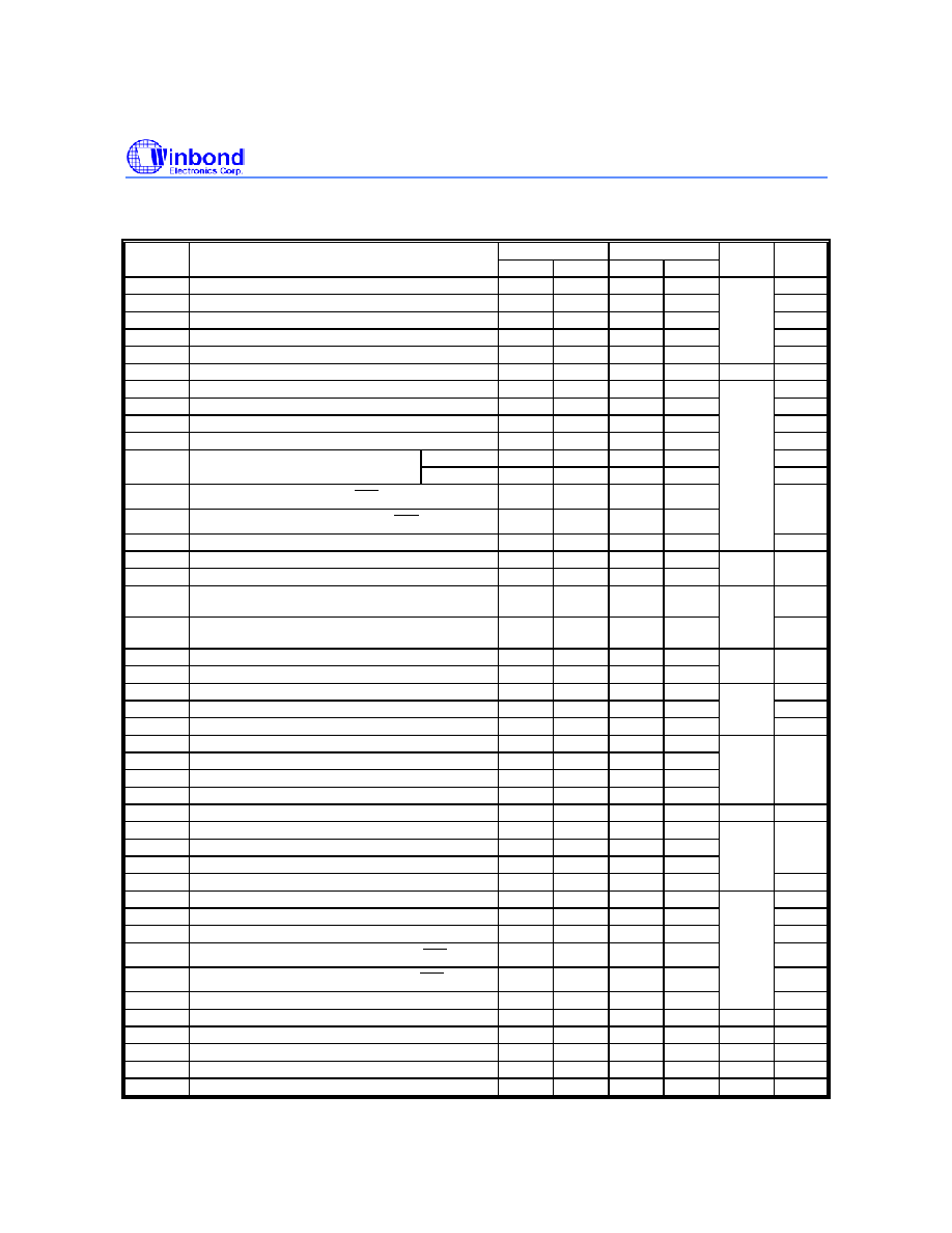
AC Characteristics and Operating Condition
(Notes: 10, 12)
-70
-75
SYM.
PARAMETER
MIN.
MAX.
MIN.
MAX.
UNITS
NOTES
tRC
Active to Ref/Active Command Period
65
tRFC
Ref to Ref/Active Command Period
75
tRAS
Active to Precharge Command Period
45
100000
45
100000
tRCD
Active to Read/Write Command Delay Time
20
tRAP
Active to Read with Auto Precharge Enable
15
nS
tCCD
Read/Write(a) to Read/Write(b) Command Period
1
tCK
tRP
Precharge to Active Command Period
20
tRRD
Active(a) to Active(b) Command Period
15
tWR
Write Recovery Time
15
tDAL
Auto Precharge Write Recovery + Precharge Time
30
CL = 2
7.5
15
8
15
tCK
CLK Cycle Time
CL = 2.5
7
15
7.5
15
tAC
Data Access Time from CLK,
CLK
-0.75
0.75
-0.75
0.75
tDQSCK
DQS Output Access Time from CLK, CLK
-0.75
0.75
-0.75
0.75
16
tDQSQ
Data Strobe Edge to Output Data Edge Skew
0.5
nS
tCH
CLk High Level Width
0.45
0.55
0.45
0.55
tCL
CLK Low Level Width
0.45
0.55
0.45
0.55
tCK
11
tHP
CLK Half Period (minimum of actual tCH, tCL)
Min.
(tCL,tCH)
Min.
(tCL,tCH)
tQH
DQ Output Data Hold Time from DQS
THP
-0.75
THP
-0.75
nS
tRPRE
DQS Read Preamble Time
0.9
1.1
0.9
1.1
tRPST
DQS Read Postamble Time
0.4
0.6
0.4
0.6
tCK
11
tDS
DQ and DM Setup Time
0.5
tDH
DQ and DM Hold Time
0.5
tDIPW
DQ and DM Input Pulse Width (for each input)
1.75
nS
tDQSH
DQS Input High Pulse Width
0.35
tDQSL
DQS Input Low Pulse Width
0.35
tDSS
DQS Falling Edge to CLK Setup Time
0.2
tDSH
DQS Falling Edge Hold Time from CLK
0.2
tCK
11
tWPRES
Clock to DQS Write Preamble Set-up Time
0
nS
tWPRE
DQS Write Preamble Time
0.25
tWPST
DQS Write Postamble Time
0.4
tDQSS
Write Command to First DQS Latching Transition
0.75
1.25
0.75
1.25
11
tDSSK
UDQS – LDQS Skew (x 16)
-0.25
0.25
-0.25
0.25
tCK
tIS
Input Setup Time
0.9
tIH
Input Hold Time
0.9
tIPW
Control & Address Input Pulse Width (for each input)
2.2
tHZ
Data-out High-impedance Time from CLK, CLK
-0.75
0.75
-0.75
0.75
tLZ
Data-out Low-impedance Time from CLK, CLK
-0.75
0.75
-0.75
0.75
tT(SS)
SSTL Input Transition
0.5
1.5
0.5
1.5
nS
tWTR
Internal Write to Read Command Delay
1
tCK
tXSNR
Exit Self Refresh to non-Read Command
75
nS
tXSRD
Exit Self Refresh to Read Command
10
tCK
tREF
Refresh Time (8k)
64
mS
tMRD
Mode Register Set Cycle Time
15
nS
相关PDF资料 |
PDF描述 |
|---|---|
| W9864G6IH-6 | 4M X 16 DDR DRAM, 5 ns, PDSO54 |
| WA-1RX33-A4 | SNAP ACTING/LIMIT SWITCH |
| WA-A325CBM | Peripheral Interface |
| WA-A325CPC | Peripheral Interface |
| WA-A325CPI | Peripheral Interface |
相关代理商/技术参数 |
参数描述 |
|---|---|
| W942508BH | 制造商:未知厂家 制造商全称:未知厂家 功能描述:DRAM |
| W942508CH | 制造商:WINBOND 制造商全称:Winbond 功能描述:8M x 4 BANKS x 8 BIT DDR SDRAM |
| W942508CH-5 | 制造商:WINBOND 制造商全称:Winbond 功能描述:8M x 4 BANKS x 8 BIT DDR SDRAM |
| W942508CH-6 | 制造商:WINBOND 制造商全称:Winbond 功能描述:8M x 4 BANKS x 8 BIT DDR SDRAM |
| W942508CH-7 | 制造商:WINBOND 制造商全称:Winbond 功能描述:8M x 4 BANKS x 8 BIT DDR SDRAM |
发布紧急采购,3分钟左右您将得到回复。