- 您现在的位置:买卖IC网 > Datasheet目录369 > W9751G6IB-25 (Winbond Electronics)IC DDR2-800 SDRAM 512MB 84-WBGA Datasheet资料下载
参数资料
| 型号: | W9751G6IB-25 |
| 厂商: | Winbond Electronics |
| 文件页数: | 10/86页 |
| 文件大小: | 0K |
| 描述: | IC DDR2-800 SDRAM 512MB 84-WBGA |
| 标准包装: | 210 |
| 格式 - 存储器: | RAM |
| 存储器类型: | DDR2 SDRAM |
| 存储容量: | 512M(32Mx16) |
| 速度: | 2.5ns |
| 接口: | 并联 |
| 电源电压: | 1.7 V ~ 1.9 V |
| 工作温度: | 0°C ~ 85°C |
| 封装/外壳: | 84-TFBGA |
| 供应商设备封装: | 84-WBGA(8x12.5) |
| 包装: | 托盘 |
第1页第2页第3页第4页第5页第6页第7页第8页第9页当前第10页第11页第12页第13页第14页第15页第16页第17页第18页第19页第20页第21页第22页第23页第24页第25页第26页第27页第28页第29页第30页第31页第32页第33页第34页第35页第36页第37页第38页第39页第40页第41页第42页第43页第44页第45页第46页第47页第48页第49页第50页第51页第52页第53页第54页第55页第56页第57页第58页第59页第60页第61页第62页第63页第64页第65页第66页第67页第68页第69页第70页第71页第72页第73页第74页第75页第76页第77页第78页第79页第80页第81页第82页第83页第84页第85页第86页
�� �
�
�W9751G6IB�
�Notes:�
�1.� To� guarantee� ODT� off,� V� REF� must� be� valid� and� a� LOW� level� must� be� applied� to� the� ODT� pin.�
�2.� V� REF� must� be� within� ±� 300� mV� with� respect� to� V� DDQ� /2� during� supply� ramp� time.�
�3.� V� DD� /V� DDL� voltage� ramp� time� must� be� no� greater� than� 200� mS� from� when� V� DD� ramps� from� 300� mV� to� V� DD� min.�
�4.� The� V� DDQ� voltage� ramp� time� from� when� V� DD� min� is� achieved� on� V� DD� to� when� V� DDQ� min� is� achieved� on� V� DDQ� must� be� no�
�greater� than� 500� mS.�
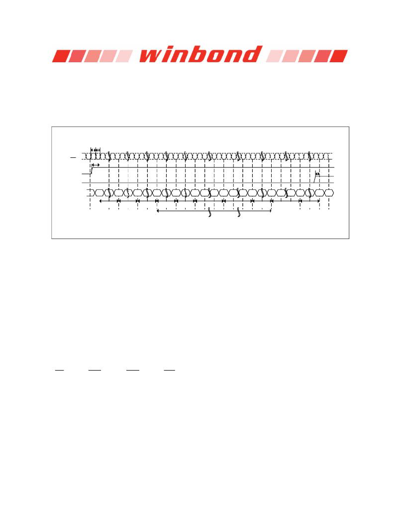
�t� CH� t� CL�
�CLK�
�CLK�
�CKE�
�ODT�
�t� IS�
�t� IS�
�Command�
�NOP�
�400nS�
�PRE�
�ALL�
�t� RP�
�EMRS�
�t� MRD�
�MRS�
�t� MRD�
�PRE�
�ALL�
�t� RP�
�REF�
�t� RFC�
�REF�
�t� RFC�
�MRS�
�t� MRD�
�EMRS�
�Follow� OCD�
�EMRS�
�t� OIT�
�ANY�
�CMD�
�DLL�
�Enable�
�DLL�
�Reset�
�min� 200� Cycle�
�OCD�
�Default�
�Flow� chart�
�OCD�
�CAL.� Mode�
�Exit�
�Figure� 1� —� Initialization� sequence� after� power-up�
�7.2�
�Mode� Register� and� Extended� Mode� Registers� Operation�
�For� application� flexibility,� burst� length,� burst� type,� CAS� Latency,� DLL� reset� function,� write� recovery�
�time� (WR)� are� user� defined� variables� and� must� be� programmed� with� a� Mode� Register� Set� (MRS)�
�command.� Additionally,� DLL� disable� function,� driver� impedance,� additive� CAS� Latency,� ODT� (On� Die�
�Termination),� single-ended� strobe� and� OCD� (off� chip� driver� impedance� adjustment)� are� also� user�
�defined� variables� and� must� be� programmed� with� an� Extended� Mode� Register� Set� (EMRS)� command.�
�Contents� of� the� Mode� Register� (MR)� or� Extended� Mode� Registers� EMR� (1),� EMR� (2)� and� EMR� (3)� can�
�be� altered� by� re-executing� the� MRS� or� EMRS� Commands.� Even� if� the� user� chooses� to� modify� only� a�
�subset� of� the� MR� or� EMR� (1),� EMR� (2)� and� EMR� (3)� variables,� all� variables� within� the� addressed�
�register� must� be� redefined� when� the� MRS� or� EMRS� commands� are� issued.�
�MRS,� EMRS� and� Reset� DLL� do� not� affect� array� contents,� which� mean� re-initialization� including� those�
�can� be� executed� at� any� time� after� power-up� without� affecting� array� contents.�
�7.2.1�
�Mode� Register� Set� Command� (MRS)�
�(� CS� =� "L",� RAS� =� "L",� CAS� =� "L",� WE� =� "L",� BA0� =� "L",� BA1� =� "L",� A0� to� A12� =� Register� Data)�
�The� mode� register� stores� the� data� for� controlling� the� various� operating� modes� of� DDR2� SDRAM.� It�
�programs� CAS� Latency,� burst� length,� burst� sequence,� test� mode,� DLL� reset,� Write� Recovery� (WR)� and�
�various� vendor� specific� options� to� make� DDR2� SDRAM� useful� for� various� applications.� The� default�
�value� in� the� Mode� Register� after� power-up� is� not� defined,� therefore� the� Mode� Register� must� be�
�programmed� during� initialization� for� proper� operation.�
�The� DDR2� SDRAM� should� be� in� all� bank� precharge� state� with� CKE� already� HIGH� prior� to� writing� into�
�the� mode� register.� The� mode� register� set� command� cycle� time� (t� MRD� )� is� required� to� complete� the� write�
�operation� to� the� mode� register.� The� mode� register� contents� can� be� changed� using� the� same� command�
�and� clock� cycle� requirements� during� normal� operation� as� long� as� all� banks� are� in� the� precharge� state.�
�The� mode� register� is� divided� into� various� fields� depending� on� functionality.� Burst� length� is� defined� by�
�A[2:0]� with� options� of� 4� and� 8� bit� burst� lengths.� The� burst� length� decodes� are� compatible� with� DDR�
�Publication� Release� Date:� Oct.� 23,� 2009�
�-� 10� -�
�Revision� A06�
�相关PDF资料 |
PDF描述 |
|---|---|
| W9751G6KB-25 | IC DDR2 SDRAM 512MBIT 84WBGA |
| W9812G6JH-6I | IC SDRAM 128MBIT 54TSOPII |
| W9816G6IH-6I | IC SDRAM 16MBIT 50TSOPII |
| W9825G6JH-6I | IC SDRAM 256MBIT 54TSOPII |
| W9864G6JH-6I | IC SDRAM 64MBIT 54TSOPII |
相关代理商/技术参数 |
参数描述 |
|---|---|
| W9751G6JB | 制造商:WINBOND 制造商全称:Winbond 功能描述:8M ? 4 BANKS ? 16 BIT DDR2 SDRAM |
| W9751G6JB-25 | 制造商:Winbond Electronics Corp 功能描述:512GB DDRII |
| W9751G6JB-3 | 制造商:Winbond Electronics Corp 功能描述:512MB DDRII |
| W9751G6KB | 制造商:WINBOND 制造商全称:Winbond 功能描述:8M ? 4 BANKS ? 16 BIT DDR2 SDRAM |
| W9751G6KB-18 | 制造商:Winbond Electronics Corp 功能描述:IC MEMORY |
发布紧急采购,3分钟左右您将得到回复。