- 您现在的位置:买卖IC网 > PDF目录203637 > W986432DH-6 (WINBOND ELECTRONICS CORP) 2M X 32 SYNCHRONOUS DRAM, 5 ns, PDSO86 PDF资料下载
参数资料
| 型号: | W986432DH-6 |
| 厂商: | WINBOND ELECTRONICS CORP |
| 元件分类: | DRAM |
| 英文描述: | 2M X 32 SYNCHRONOUS DRAM, 5 ns, PDSO86 |
| 封装: | 0.400 INCH, 0.50 MM PITCH, TSOP2-86 |
| 文件页数: | 44/48页 |
| 文件大小: | 1648K |
| 代理商: | W986432DH-6 |
第1页第2页第3页第4页第5页第6页第7页第8页第9页第10页第11页第12页第13页第14页第15页第16页第17页第18页第19页第20页第21页第22页第23页第24页第25页第26页第27页第28页第29页第30页第31页第32页第33页第34页第35页第36页第37页第38页第39页第40页第41页第42页第43页当前第44页第45页第46页第47页第48页
W986432DH
Publication Release Date: July 30, 2002
- 5 -
Revision A5
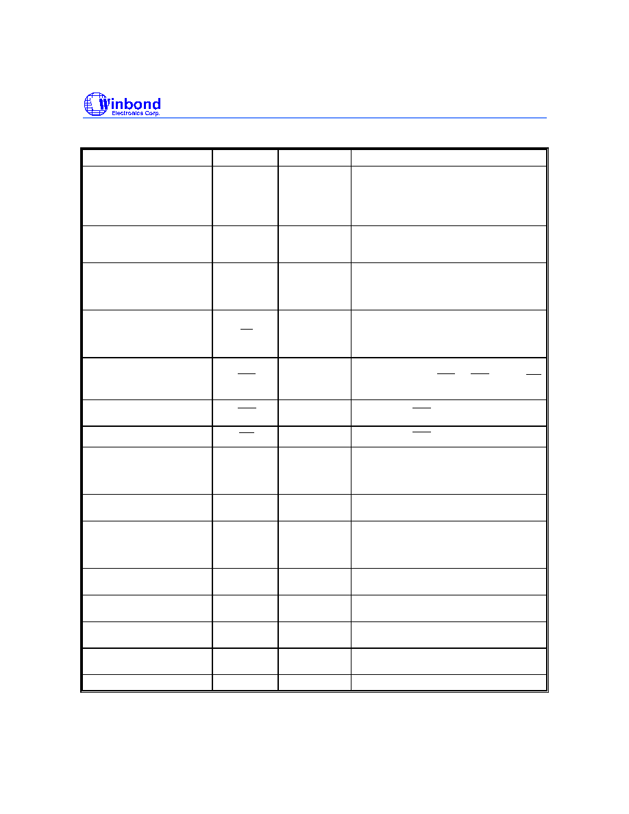
5. PIN DESCRIPTION
PIN NUMBER
PIN NAME
FUNCTION
DESCRIPTION
24, 25, 26, 27, 60,
61, 62, 63, 64, 65, 66
A0
A10
Address
Multiplexed pins for row and column address.
Row address: A0
A10. Column address:
A0
A7. A10 is sampled during a precharge
command to determine if all banks are to be
precharged or bank selected by BS0, BS1.
22, 23
BS0, BS1
Bank Select
Select bank to activate during row address
latch time, or bank to read/write during
address latch time.
2, 4, 5, 7, 8, 10, 11, 13, 31,
33, 34, 36, 37, 39, 40, 42, 45,
47, 48, 50, 51, 53, 54, 56, 74,
76, 77, 79, 80, 82, 83, 85
DQ0
DQ31
Data Input/
Output
Multiplexed pins for data output and input.
20
CS
Chip Select
Disable or enable the command decoder.
When command decoder is disabled, new
command is ignored and previous operation
continues.
19
RAS
Row Address
Strobe
Command input. When sampled at the rising
edge of the clock
RAS ,
CAS
and
WE
define the operation to be executed.
18
CAS
Column
Address Strobe Referred to
RAS
17
WE
Write Enable
Referred to
RAS
16, 28, 59, 71
DQM0
DQM3
Input/Output
Mask
The output buffer is placed at Hi-Z (with
latency of 2) when DQM is sampled high in
read cycle. In write cycle, sampling DQM high
will block the write operation with zero latency.
68
CLK
Clock Inputs
System clock used to sample inputs on the
rising edge of clock.
67
CKE
Clock Enable
CKE controls the clock activation and
deactivation. When CKE is low, Power Down
mode, Suspend mode, or Self Refresh mode
is entered.
1, 15, 29, 43
VCC
Power (+3.3V)
Power for input buffers and logic circuit inside
DRAM.
44, 58, 72, 86
VSS
Ground
Ground for input buffers and logic circuit
inside DRAM.
3, 9, 35, 41, 49, 55, 75, 81
VCCQ
Power (+3.3V)
for I/O Buffer
Separated power from VCC, to improve DQ
noise immunity.
6, 12, 32, 38, 46, 52, 78, 84
VSSQ
Ground for I/O
Buffer
Separated ground from VSS, to improve DQ
noise immunity.
14, 21, 30, 57, 69, 70, 73
NC
No Connection
No connection
相关PDF资料 |
PDF描述 |
|---|---|
| W986432DH-8 | 2M X 32 SYNCHRONOUS DRAM, 6 ns, PDSO86 |
| W987Z6CBG80 | 8M X 16 SYNCHRONOUS DRAM, 6 ns, PBGA54 |
| WA-1RVX051-A4 | SNAP ACTING/LIMIT SWITCH |
| WA-1RX12-A4 | SNAP ACTING/LIMIT SWITCH |
| WB3M200VD1R800 | 200 CONTACT(S), MALE, STRAIGHT SINGLE PART CARD EDGE CONN, SURFACE MOUNT, PLUG |
相关代理商/技术参数 |
参数描述 |
|---|---|
| W986432DH-6I | 制造商:未知厂家 制造商全称:未知厂家 功能描述:SDRAM|4X512KX32|CMOS|TSSOP|86PIN|PLASTIC |
| W986432DH-7 | 制造商:未知厂家 制造商全称:未知厂家 功能描述:SDRAM|4X512KX32|CMOS|TSSOP|86PIN|PLASTIC |
| W986432DH-7L | 制造商:未知厂家 制造商全称:未知厂家 功能描述:SDRAM|4X512KX32|CMOS|TSSOP|86PIN|PLASTIC |
| W9864G2DH6 | 制造商:WINBOND 功能描述:New |
| W9864G2GH | 制造商:WINBOND 制造商全称:Winbond 功能描述:512K X 4 BANKS X 32BITS SDRAM |
发布紧急采购,3分钟左右您将得到回复。