- 您现在的位置:买卖IC网 > PDF目录140424 > WED2DL32512V40BI 512K X 32 MULTI DEVICE SRAM MODULE, 4 ns, PBGA119 PDF资料下载
参数资料
| 型号: | WED2DL32512V40BI |
| 元件分类: | SRAM |
| 英文描述: | 512K X 32 MULTI DEVICE SRAM MODULE, 4 ns, PBGA119 |
| 封装: | PLASTIC, BGA-119 |
| 文件页数: | 5/9页 |
| 文件大小: | 143K |
| 代理商: | WED2DL32512V40BI |
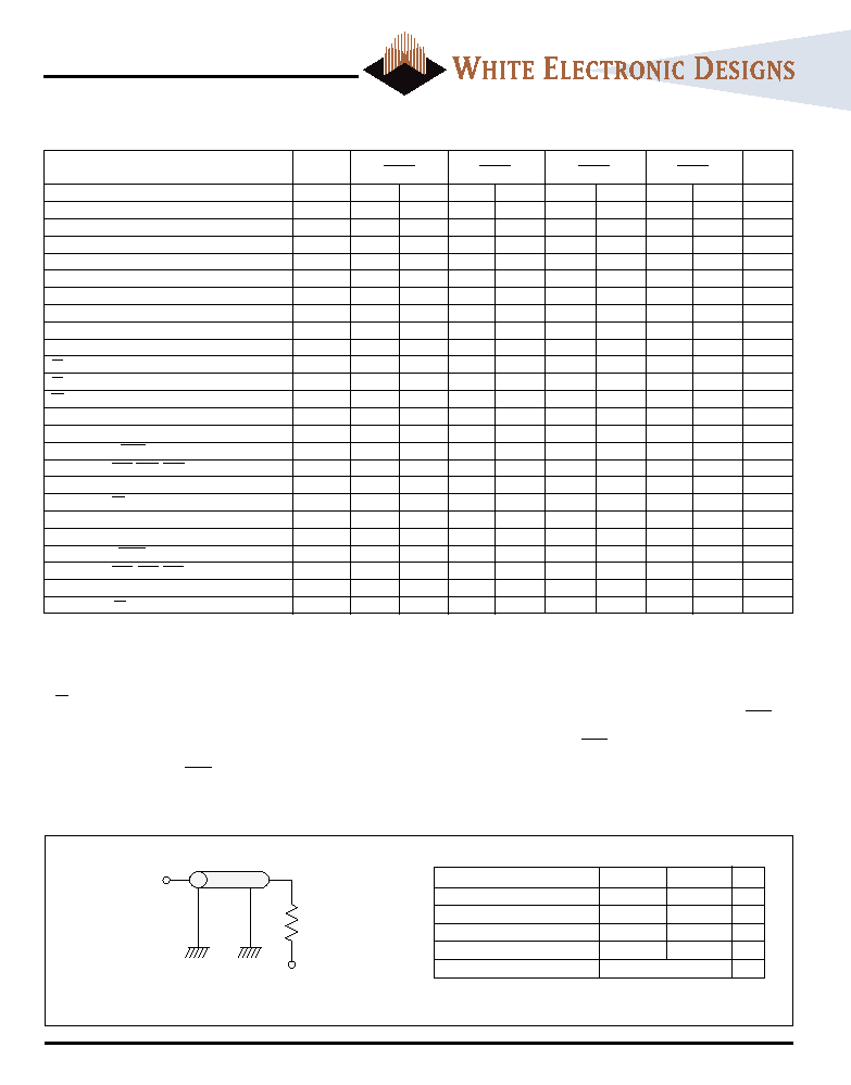
5
White Electronic Designs Corporation (508) 366-5151 www.whiteedc.com
WED2DL32512V
AC CHARACTERISTICS
Symbol
200MHz
166MHz
150MHz
133MHz
Parameter
Min
Max
Min
Max
Min
Max
Min
Max
Units
Clock
Clock Cycle Time
tKC
5.0
6.0
6.6
7.5
ns
Clock Frequency
tKF
200
166
150
133
MHz
Clock HIGH Time
tKH
2.0
2.4
2.6
ns
Clock LOW Time
tKL
2.0
2.4
2.6
ns
Output Times
Clock to output valid
tKQ
2.5
3.5
3.8
4.0
ns
Clock to output invalid (2)
tKQX
1.5
1.25
1.5
ns
Clock to output on Low-Z (2,3,4)
tKQLZ
00
ns
Clock to output in High-Z (2,3,4)
tKQHZ
3.0
3.5
3.8
4.0
ns
OE to output valid (5)
tOEQ
2.5
3.5
3.8
4.0
ns
OE to output in Low-Z (2,3,4)
tOELZ
00
ns
OE to output in High Z (2,3,4)
tOEHZ
2.5
3.5
3.8
4.0
ns
Setup Times
Address (6,7)
tAS
1.5
ns
Address status (ADSC) (6,7)
tADSS
1.5
ns
Write signals (BWa-BWd, BWE) (6,7)
tWS
1.5
ns
Data-in (6,7)
tDS
1.5
ns
Chip enables (CE) (6,7)
tCES
1.5
ns
Hold Times
Address (6,7)
tAH
0.5
ns
Address status (ADSC) (6,7)
tADSH
0.5
ns
Write Signals (BWa-BWd, BWE) (6,7)
tWH
0.5
ns
Data-in (6,7)
tDH
0.5
ns
Chip Enables (CE) (6,7)
tCEH
0.5
ns
NOTES:
1. Test conditions as specified with the output loading as shown in Figure 1 for 3.3V 1/0 and Figure 3 for 2.5V 1/0 unless otherwise noted.
2. This parameter is measured with output load as shown in Figure 2 for 3.3V 1/0 and Figure 4 for 2.5V 1/0.
3. This parameter is sampled.
4. Transition is measured
±500mV from steady state voltage.
5. OE is a “Don’t Care” when a byte write enable is sampled LOW.
6. A WRITE cycle is defined by at least one byte write enable LOW for the required setup and hold times. A READ cycle is defined by all byte write enables HIGH and ADSC
LOW for the required setup and hold times.
7. This is a synchronous device. All addresses must meet the specified setup and hold times for all rising edges of CLK when ADSC is LOW and chip enabled. All other
synchronous inputs must meet the setup and hold times with stable logic levels for all rising edges of clock (CLK) when the chip is enabled. Chip enable must be valid at
each rising edge of CLK when ADSC is LOW to remain enabled.
OUTPUT LOADS
AC TEST CONDITIONS
50
Vt = 1.5V
Output
Z0 = 50
Z0 = 50
Parameter
3.3V I/O
2.5V I/O
Unit
Input Pulse Levels
VSS to 3.0
VSS to 2.5
V
Input Rise and Fall Times
1
ns
Input Timing Reference Levels
1.5
1.25
V
Output Timing Reference Levels
1.5
1.25
V
Output Load
See figure, at left
AC Output Load Equivalent
Vt = 1.5V for 3.3V I/O
Vt = 1.25V for 2.5V I/O
相关PDF资料 |
PDF描述 |
|---|---|
| WMF128K8-120FFQ5A | 128K X 8 FLASH 5V PROM, 120 ns, CDSO32 |
| WS512K32N-100H2M | 2M X 8 MULTI DEVICE SRAM MODULE, 100 ns, CPGA66 |
| WS1M8-55CC | 1M X 8 STANDARD SRAM, 55 ns, CDIP32 |
| WS512K32F-35G4TI | 2M X 8 MULTI DEVICE SRAM MODULE, 35 ns, QMA68 |
| WS512K32F-55G4TC | 2M X 8 MULTI DEVICE SRAM MODULE, 55 ns, QMA68 |
相关代理商/技术参数 |
参数描述 |
|---|---|
| WED2DL32512V-B | 制造商:未知厂家 制造商全称:未知厂家 功能描述:SSRAM MCP |
| WED2DL32512V-BC | 制造商:未知厂家 制造商全称:未知厂家 功能描述:TMS320C6202. TMS320C6203. TMS320C6204. TMS320C6 Families |
| WED2DL36513V-B | 制造商:未知厂家 制造商全称:未知厂家 功能描述:SSRAM MCP |
| WED2EG472512V5D2 | 制造商:WEDC 制造商全称:White Electronic Designs Corporation 功能描述:16MB (4x512Kx72) SYNC BURST PIPELINE, DUAL KEY DIMM |
| WED2EG472512V65D2 | 制造商:WEDC 制造商全称:White Electronic Designs Corporation 功能描述:16MB (4x512Kx72) SYNC BURST PIPELINE, DUAL KEY DIMM |
发布紧急采购,3分钟左右您将得到回复。