参数资料
| 型号: | X9252YV24IZ-2.7 |
| 厂商: | Intersil |
| 文件页数: | 2/20页 |
| 文件大小: | 0K |
| 描述: | IC POT DGTL QUAD 24-TSSOP |
| 标准包装: | 62 |
| 系列: | XDCP™ |
| 接片: | 256 |
| 电阻(欧姆): | 2.8k |
| 电路数: | 4 |
| 温度系数: | 标准值 ±300 ppm/°C |
| 存储器类型: | 非易失 |
| 接口: | I²C(芯片选择,设备位址,增/减) |
| 电源电压: | 2.7 V ~ 5.5 V |
| 工作温度: | -40°C ~ 85°C |
| 安装类型: | 表面贴装 |
| 封装/外壳: | 24-TSSOP(0.173",4.40mm 宽) |
| 供应商设备封装: | 24-TSSOP |
| 包装: | 管件 |
| 产品目录页面: | 1237 (CN2011-ZH PDF) |
10
FN8167.2
November 14, 2005
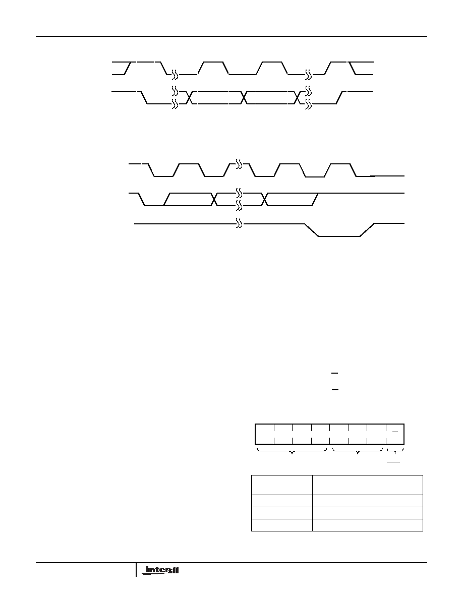
Serial Acknowledge
An ACK (Acknowledge), is a software convention used to
indicate a successful data transfer. The transmitting device,
either master or slave, releases the bus after transmitting
eight bits. During the ninth clock cycle, the receiver pulls the
SDA line LOW to acknowledge the reception of the eight bits
of data (See Figure 3).
The device responds with an ACK after recognition of a
START condition followed by a valid Slave Address byte. A
valid Slave Address byte must contain the Device Type
Identifier 0101, and the Device Address bits matching the
logic state of pins A2, A1, and A0 (See Figure 4).
If a write operation is selected, the device responds with an
ACK after the receipt of each subsequent eight-bit word.
In the read mode, the device transmits eight bits of data,
releases the SDA line, and then monitors the line for an
ACK. The device continues transmitting data if an ACK is
detected. The device terminates further data transmissions if
an ACK is not detected. The master must then issue a STOP
condition to place the device into a known state.
Slave Address Byte
Following a START condition, the master must output a Slave
Address Byte (Refer to figure 4.). This byte includes three parts:
- The four MSBs (SA7-SA4) are the Device Type Identifier,
which must always be set to 0101 in order to select the
X9252.
- The next three bits (SA3-SA1) are the Device Address bits
(AS2-AS0). To access any part of the X9252’s memory,
the value of bits AS2, AS1, and AS0 must correspond to
the logic levels at pins A2, A1, and A0 respectively.
- The LSB (SA0) is the R/W bit. This bit defines the
operation to be performed on the device being
addressed. When the R/W bit is “1”, then a Read
operation is selected. A “0” selects a Write operation
.
SDA
SCL
START
DATA
STOP
STABLE
CHANGE
DATA
STABLE
FIGURE 2. VALID DATA CHANGES, START, AND STOP CONDITIONS
SDA Output from
Transmitter
SDA Output from
Receiver
8
1
9
START
ACK
SCL from Master
FIGURE 3. ACKNOWLEDGE RESPONSE FROM RECEIVER
SA6
SA7
SA5
SA3
SA2
SA1
SA0
Device Type
Identifier
Read or
SA4
SLAVE ADDRESS
BIT(S)
DESCRIPTION
SA7-SA4
Device Type Identifier
SA3-SA1
Device Address
SA0
Read or Write Operation Select
R/W
01
0
1
Address
Device
AS0
AS1
AS2
Write
FIGURE 4. SLAVE ADDRESS (SA) FORMAT
X9252
相关PDF资料 |
PDF描述 |
|---|---|
| VE-B30-MV | CONVERTER MOD DC/DC 5V 150W |
| VE-J5K-MZ | CONVERTER MOD DC/DC 40V 25W |
| VI-J2Y-MZ | CONVERTER MOD DC/DC 3.3V 16.5W |
| MS3124E12-8PW | CONN RCPT 8POS JAM NUT W/PINS |
| VE-J5H-MZ | CONVERTER MOD DC/DC 52V 25W |
相关代理商/技术参数 |
参数描述 |
|---|---|
| X9258 | 制造商:INTERSIL 制造商全称:Intersil Corporation 功能描述:Low Noise/Low Power/2-Wire Bus/256 Taps |
| X9258)06 | 制造商:INTERSIL 制造商全称:Intersil Corporation 功能描述:Quad Digital Controlled Potentiometers |
| X9258_11 | 制造商:INTERSIL 制造商全称:Intersil Corporation 功能描述:Quad Digital Controlled Potentiometers(XDCP?) |
| X9258_13 | 制造商:INTERSIL 制造商全称:Intersil Corporation 功能描述:Low Noise/Low Power/2-Wire Bus/256 Taps |
| X9258TB24 | 制造商:XICOR 制造商全称:Xicor Inc. 功能描述:Quad Digital Controlled Potentiometers (XDCP) |
发布紧急采购,3分钟左右您将得到回复。