参数资料
| 型号: | X9252YV24IZ-2.7 |
| 厂商: | Intersil |
| 文件页数: | 5/20页 |
| 文件大小: | 0K |
| 描述: | IC POT DGTL QUAD 24-TSSOP |
| 标准包装: | 62 |
| 系列: | XDCP™ |
| 接片: | 256 |
| 电阻(欧姆): | 2.8k |
| 电路数: | 4 |
| 温度系数: | 标准值 ±300 ppm/°C |
| 存储器类型: | 非易失 |
| 接口: | I²C(芯片选择,设备位址,增/减) |
| 电源电压: | 2.7 V ~ 5.5 V |
| 工作温度: | -40°C ~ 85°C |
| 安装类型: | 表面贴装 |
| 封装/外壳: | 24-TSSOP(0.173",4.40mm 宽) |
| 供应商设备封装: | 24-TSSOP |
| 包装: | 管件 |
| 产品目录页面: | 1237 (CN2011-ZH PDF) |
13
FN8167.2
November 14, 2005
DCP Addressing for 2-Wire Interface
Once the register number has been selected by a 2-wire
instruction, then the DCP number is determined by the
Address Byte of the following instruction. Note again that this
enables a complete page write of the DRs of all four
potentiometers at once. The register addresses accessible
in the X9252 include:
All other address bits in the Address Byte must be set to “0”
during 2-wire write operations and their value should be
ignored when read.
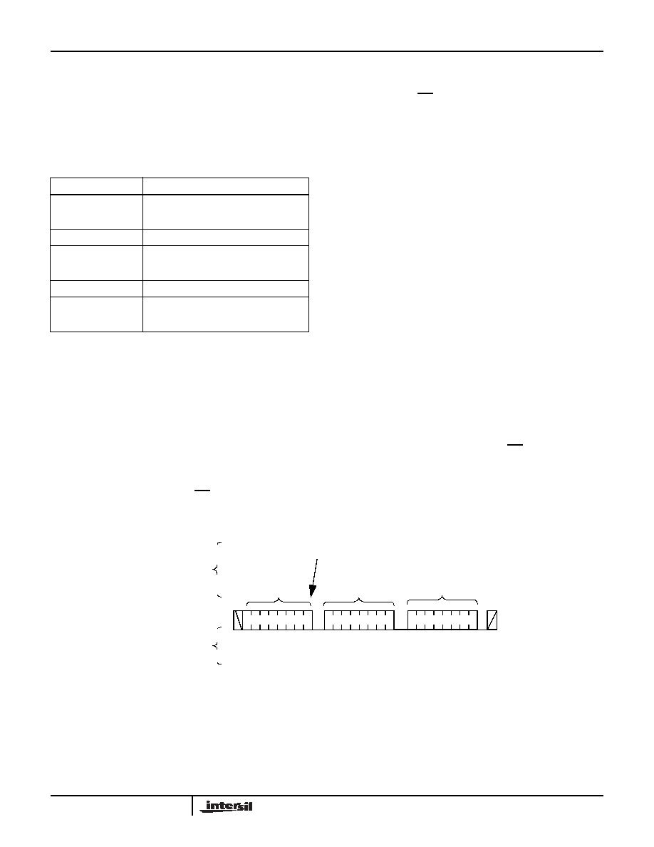
Byte Write Operation
For any Byte Write operation, the X9252 requires the Slave
Address byte, an Address Byte, and a Data Byte (See Figure
7). After each of them, the X9252 responds with an ACK.
The master then terminates the transfer by generating a
STOP condition. At this time, if the write operation is to a
volatile register (WCR, or SR), the X9252 is ready for the
next read or write operation. If the write operation is to a
nonvolatile register (DR), and the WP pin is high, the X9252
begins the internal write cycle to the nonvolatile memory.
During the internal nonvolatile write cycle, the X9252 does
not respond to any requests from the master. The SDA
output is at high impedance.
The SR bits and WP pin determine the register being
accessed through the 2-wire interface (See Table 2).
As noted before, any write operation to a Data Register
(DR), also transfers the contents of all the data registers in
that row to their corresponding WCR.
For example, to write 3Ahex to the Data Register 1 of DCP2
the following sequence is required:
During the sequence of this example, WP pin must be high,
and A0, A1, and A2 pins must be low. When completed, the
DR21 register and the WCR2 will be set to 3Ah and the other
Data Register in Row 1 will transfer their other contents to
the respective WCR’s.
TABLE 3. 2-WIRE INTERFACE ADDRESS BYTE
ADDRESS (HEX)
CONTENTS
0
DCP 0
1
DCP 1
2
DCP 2
3
DCP 3
4
Not Used
5
Not Used
6
Not Used
7
Status Register
START
Slave Address
0101 0000
ACK
Address Byte
0000 0111
ACK
Data Byte
0000 0011
ACK
note: at this ACK, the WCRs are all updated with their respective DR.
STOP
START
Slave Address
0101 0000
ACK
Address Byte
0000 0010
ACK
Data Byte
0011 1010
ACK
STOP
(Hardware Address = 000,
and a Write command)
(Indicates Status Register
address)
(Data Register 1 and
NVEnable selected)
(Hardware address = 000,
(Access DCP2)
(Write Data Byte 3Ah)
Write command)
S
t
a
r
t
S
t
o
p
Slave
Address
Byte
Data
Byte
A
C
K
Signals from the
Master
Signals from the
Slave
A
C
K
0
11
A
C
K
Write
Signal at SDA
FIGURE 7. BYTE WRITE SEQUENCE
X9252
相关PDF资料 |
PDF描述 |
|---|---|
| VE-B30-MV | CONVERTER MOD DC/DC 5V 150W |
| VE-J5K-MZ | CONVERTER MOD DC/DC 40V 25W |
| VI-J2Y-MZ | CONVERTER MOD DC/DC 3.3V 16.5W |
| MS3124E12-8PW | CONN RCPT 8POS JAM NUT W/PINS |
| VE-J5H-MZ | CONVERTER MOD DC/DC 52V 25W |
相关代理商/技术参数 |
参数描述 |
|---|---|
| X9258 | 制造商:INTERSIL 制造商全称:Intersil Corporation 功能描述:Low Noise/Low Power/2-Wire Bus/256 Taps |
| X9258)06 | 制造商:INTERSIL 制造商全称:Intersil Corporation 功能描述:Quad Digital Controlled Potentiometers |
| X9258_11 | 制造商:INTERSIL 制造商全称:Intersil Corporation 功能描述:Quad Digital Controlled Potentiometers(XDCP?) |
| X9258_13 | 制造商:INTERSIL 制造商全称:Intersil Corporation 功能描述:Low Noise/Low Power/2-Wire Bus/256 Taps |
| X9258TB24 | 制造商:XICOR 制造商全称:Xicor Inc. 功能描述:Quad Digital Controlled Potentiometers (XDCP) |
发布紧急采购,3分钟左右您将得到回复。